LMK04828: ADC, DAC and LMK with Agilex 5 device

Part Number: LMK04828
Other Parts Discussed in Thread: ADC12QJ1600

Tool/software:

Hi Team, 


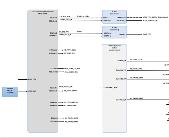
I want to interface the LMK04828B Clock Generator, ADC12QJ1600AAVQ1: Analog to Digital Converter (ADC), and DAC37J84IAAV: Digital to Analog Converter (DAC) with the Altera Agilex 5 device.
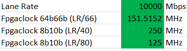
May I know what will be the clock requirements, such as device clock and sysref for ADC and DAC? As well as what is the range of clock frequencies that needs to be supported for FPGA reference clocks.

Regards,
Liston

  • Hi Liston, 

    This thread is currently assigned to the clocks and timing group, I'll go ahead and redirect it to the high-speed data converters group so they can answer your questions. 

    Regards, 

    Connor 

  • Hi Liston,

    Please be more specific on the clocking requirements.

    What sampling rate do you plan to use?

    It might be easier to guide you if you can send us a block diagram on your proposed setup of both the ADC and DAC.

    Please advise.

    Regards,

    Rob


  • Above is the block diagram for the same.
    Sampling rate is around 1GSPS.
    The SYSREF for ADC and DAC, FPGA Core clock and sysref for the Agilex 5 FPGA as well as REF Clocks for the Transceiver Banks. For these values are there any calculations or reference.

  • Hi Liston,

    Your sampling rate for both the ADC and DAC is 1GSPS?

    What modes settings do you plan to use both the ADC and DAC?

    This would give you an understanding of the FPGA clocking requirements. This information is provided in the datasheet.

    Regards,

    Rob

  • Hi Rob,

    For ADC: JMODE 0 (LMF = 888)
    For DAC: LMF = 841
    These would be the mode settings for the ADC and DAC.

    Regards,
    Liston

  • Hi Rob, Any updates on this?

    For ADC: JMODE 0 (LMF = 888)
    For DAC: LMF = 841
    These would be the mode settings for the ADC and DAC.

    Regards,
    Liston

  • Hi Liston,

    The datasheet should have all the necessary information in order to calculate the FPGA clocks, etc.

    However, I have this generic spreadsheet that might help understand this quicker based on your specific config.

    Please see attached.

    Regards,

    Rob

    Lane Rate Calc GUI.xlsx

  • Hi Rob,

    Thanks for the support.
    what is the decimation or DDC factor and how to calculate it.

    Regards,
    Liston

  • Hi Rob, 

    In the Lane rate calculation excel sheet, there is the formula as follows:
    Lane Rate = ((Sampling Frequency)/(decimation))*(#bits/sample)*(encoding) * (I/Q Channels) * (# of Channels) / (#lanes)

    In the datasheet, the line rate formula is given as follows:.
    f(LINERATE) = fS x R

    Can you explain the line rate calculation for JMODE=0? 

    Regards,
    Liston

  • Hi Liston,

    Please see pages 80 and 81 of the ADC12QJ1600 datasheet.

    Regards,

    Rob

  • Hi Rob,

    The FPGA Clock Calculation from the Excel that you shared has separate formulas as mentioned below.

    For 8b/10b, there are 2 separate values: LR/40 and LR/80. Could you please explain this?

    Regards,
    Liston

  • Liston,

    Some customer use a line rate of /40 or /80 for the FPGA clock, this is your choice on how you implement the FPGA FW.

    Regards,

    Rob