Other Parts Discussed in Thread: LMK5B33216, USB2ANY
Tool/software:
before:
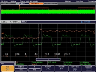
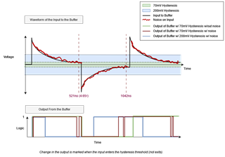
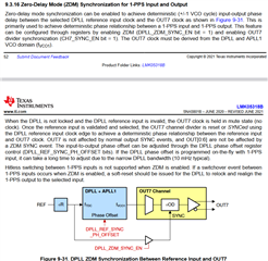
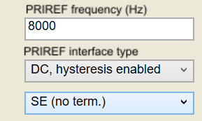
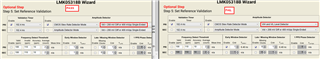
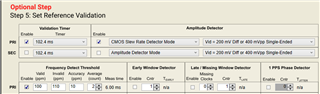
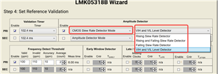
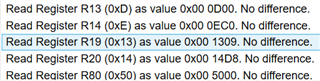
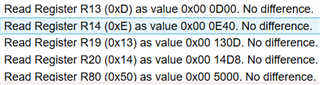
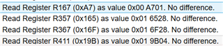
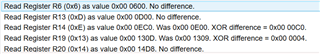
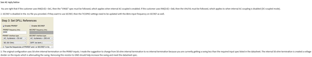
The 05318b used in our project is used as the jitter cleaner chip, with the input ref clk = 8kHz, the output out7 24.576MHz, the input mode is configured in DC mode, the corresponding register is reg40 0x07, and the register reg46 0x1c, indicating single-ended(internal termination 50 Ω). Since it is DC mode, the pin PRIREF_P of the 05318b chip is about 1.3V, and non-1.8V is at risk of being identified as low level. But the clock phases of he input and ouput are synchronized, it has no noise in audio channel.
after:
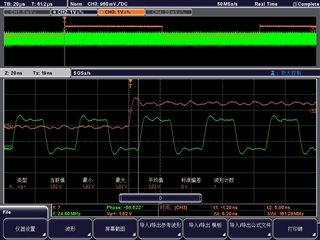
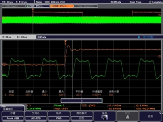
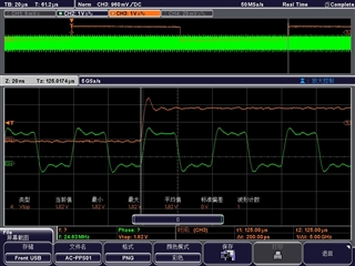
We configured according to the recommended configuration of TI engineers, modify the register reg40 to 0x03 AC coupled internally and reg46 to 0x18, indicating CMOS. And the PRIREF_P pin of the chip is 1.8V, but we found that the clock phases of the input and output are not synchronized, which also causes noise to be made on the audio channel we finally output.
question:
We want to know why the clock phases of the input and output are not synchronized when we change the dc mode to ac mode, and how to solve this problem and change clock phase to be synchronized.