This thread has been locked.

If you have a related question, please click the "Ask a related question" button in the top right corner. The newly created question will be automatically linked to this question.

LMX2492EVM: External VCO and D1 LED

Part Number: LMX2492EVM

Tool/software:

Hi TI forum,

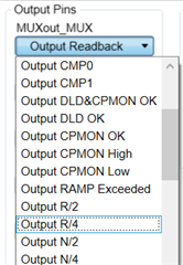
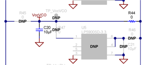
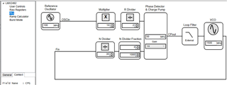
I have just connected an external VCO by removing R6 and R4_LF, and connecting RF_out's SMA to VCO RF_out divided by 16 (24 GHz VCO to 1.5 GHz DIV) and Valf to VCO's Vtune. Also I have changed the values of the passive filter using PLLatinum SIM. In TICS Pro I have configured the PLL tab like this:


VCO output is -10 dBm, but from what I have read in this thread is fine (https://e2e.ti.com/support/clock-timing-group/clock-and-timing/f/clock-timing-forum/742862/lmx2492-power-level-for-fin?tisearch=e2e-sitesearch&keymatch=LMX2492%25252525252520fin#). And, Vtune, has a range from 0 V to 1.8 V. 

VCO just connected and without Vtune voltage operates at 1.387 GHz, but the desired frequency is 1.5 GHz, and my objective is to do ramps from 1.5 to 1.516 GHz.

When running that configuration, D1 LED doesn't turn on and PLL doesn't generate the 0.88 V needed to set the VCO frequency to 1.5 GHz. Also, Vtune is a flat signal at 0 V with random peaks of 1.8 V 

I would like to know if any other configuration is needed to configure the PLL to work as expected.

I can share more info if needed.

Thanks in advance,

Joaquín

  • Hi Joaquin,

    Your charge pump gain is 1x, is your loop filter design based on this current?

    To debug, you can set one of the output pins as R/2 and N/2. If it is locked, you should get 25MHz (fpd / 2). 

  • Hi Noel,

    The design in PLLatinum SIM was calculated using 3.1 Kpd, but in order to protect the VCO I have reduced it to x1 so the peaks it generates don't go over 1.8 V.

    For testing I have been using D1 only for DLD OK to check PLL's capability to lock with the signal, do you recommend more to use R/2 or N/2? Aside from the preferred LED config, I couldn't get a green light from the PLL even when using an spectrum analyzer's TG. I have check the LED if it can turn on but I can't understand why it doesn't work when reading from Fin*. Other metric I'm looking while trying to figure out why PLL doesn't work as expected is Vtune. I'm using and osciloscope and looking for when the CP change from low to high as a way to help me find where the lock of the signal could be found, but for a 1.5 GHz signal it is arround 3.05 GHz.

    Could it be something wrong with the modifications we did in the circuit? Is there any other metric I can measure in order to understand what is going on with the PLL?


    Best regards,

    Joaquín

  • Hi Joaquin,

    3.1 Kpd --> 3.1mA; x1 --> 0.1mA. This is a huge different, can you confirm your loop filter is still stable at x1?

    Settings R/2 and N/2 are used to debug, not for normal use. If the input path is normal, you should get stable 25MHz clock from R/2. If the VCO is lock, you should also get 25MHz clock from N/2. If the VCO is unlock, you should get some other frequency. 

  • Hi Noel,

    I’ve checked the behavior in PLLatinum Sim by adjusting the Kpd value, and while the simulation doesn’t indicate instability, there is some noticeable non-linearity.

    Additionally, I tested both R/2 and N/2. When checking R/2 on the oscilloscope, I obtained a clean 25 MHz signal, which confirms that the issue is not related to the XOSC on the LMX2492EVM. However, when measuring N/2, I observed fluctuating values between 13 MHz and 110 MHz.

    Interestingly, if I open the loop and inject a 1.5 GHz signal using a tracking generator instead of using the VCO, the N/2 output varies depending on the input signal power. For example:

    • At -10 dBm → 25 MHz

    • At -5 dBm → 15.5 MHz

    • At 0 dBm → 11.7 MHz

    Is this behavior considered normal?

    Since my VCO outputs at around -10 dBm, which is below the recommended input level, should I consider modifying the PLL's input connection to the SMA port? With the tracking generator, the R/2 output appears stable — likely due to its tunable power and low noise — but my VCO not only introduces more noise, it also introduces response delay because it uses a counter to divide the 24 GHz down to 1.5 GHz. Could this delay be causing the issue?

    Additionally, when I check the DIV output on a spectrum analyzer, I do see it at 1500 ± 2 MHz. However, the PLL doesn’t lock to it within that range and instead seems to lock onto signals around 6755 MHz or 8200 MHz. Could this be due to coupling in another part of the circuit or perhaps a faulty connection?

    Thank you very much for your insights and support.

    Best regards,
    Joaquín

  • Interesting finding, I will take a look in the lab in next week.

  • Hi Joaquin,

    Forgotten to ask, did you remove R44 to cutoff the power supply to the onboard VCO U2?

    I can get correct N/2 frequency with -29dBm 1.5GHz input to RFout connector. I was lazy, I did not remove R6 and R4_LF.

  • Hi Noel,

    We hadn’t removed it initially — but after doing so, the PLL finally locked on!

    Yesterday, we spent some time investigating why the PLL only worked when the VCO input power was removed. We found that R6 was not fully disconnected — it was just turned to the left, cutting it off from the SMA input, but still connected to the VCO output, and effectively left in parallel with R7. This unintentionally created a capacitive path that filtered noise and introduced periodic jitter, due to the interaction between the two signals: Vp at 9.6 GHz from the VCO and Vn at 1.5 GHz from the external VCO or tracking generator.

    Honestly, I would never have figured this out without your help — thank you so much for your expertise and (in this case, very helpful!) laziness!

    Best regards,
    Joaquín