This thread has been locked.

If you have a related question, please click the "Ask a related question" button in the top right corner. The newly created question will be automatically linked to this question.

LMK03328: Jitter Performance of LMK03328 as REFCLK for Artix-7 GTP Transmitter

Guru 12065 points
Part Number: LMK03328
Other Parts Discussed in Thread: CDC6C, LMH1983

Tool/software:

Hi,

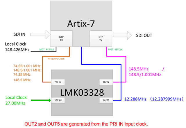
We are currently considering using your device LMK03328 in combination with Xilinx Artix-7 FPGA.

The system is intended to operate as follows:

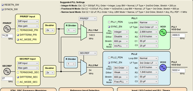
  • Input clock (recovered clock): 74.25MHz, 74.25/1.001MHz, 148.5MHz, 148.5/1.001MHz

  • LMK03328 is used for jitter cleaning and clock generation. The output clocks are:

    • 148.5MHz or 148.5/1.001MHz (used as REFCLK for Artix-7 GTP transmitter)

    • 12.288MHz (for audio clock)

We are aware that the GTP transceivers on Artix-7 have stringent phase noise / jitter mask requirements for the REFCLK.

Could you please confirm whether there are any concerns or limitations when using LMK03328 in this configuration?
Particularly, we would like your opinion on whether the jitter performance of the 148.5MHz (or 148.5/1.001MHz) output is suitable to meet the GTP transceiver’s REFCLK requirement.

Best regards,

Conor

  • Conor,

    I have a few questions here:

    1. Are you saying that the LMK03328 would need to be able to accept an input of either 148.5MHz or 74.25MHz dynamically? Or would they only need one of these two frequencies (and the F/1.001) in the system?
    2. Must the 12.288MHz clock be generated by the LMK03328? Or can this be generated by another device, such as CDC6C?
    3. Do you have the phase noise requirements available that you can share?

    Thanks,

    Kadeem

  • Hi Kadeem,

    Thank you for your follow-up. Please see below the our responses to your questions:

    1. Input Clock Switching Behavior
    The recovered clock frequency is selected dynamically according to the SDI video input format, as shown below:

    1080i59.94, 1080p29.97 → 74.25 / 1.001 MHz

    1080p59.94 → 148.5 / 1.001 MHz

    1080i50, 1080p25, 1080i60, 1080p30 → 74.25 MHz

    1080p50, 1080p60 → 148.5 MHz

    The LMK03328 will need to accept one of these input clock frequencies depending on the input format.
    Dynamic switching occurs only when the SDI video format changes. During normal operation, the system is locked to a single input bit rate, so the input clock remains fixed unless the video format is changed.

    The 148.5 MHz or 148.5 / 1.001 MHz clock generated from the recovered clock will be used as the REFCLK for the GTP transmitter in the Artix-7 FPGA.

    2. 12.288 MHz Audio Clock Generation
    The 12.288 MHz audio clock must be generated by the LMK03328.
    Due to input clock frequency and internal VCO operating constraints, the actual output frequency will be 12.287999 MHz.


    3. Artix-7 GTP REFCLK Jitter Requirement
    We are referring to Xilinx Answer Record AR#44549 – "7 Series FPGA GTX_GTH_GTP Transceivers - Reference Clock Phase Noise Masks" as the reference for the GTP transceiver’s REFCLK jitter and phase noise requirements.

    Please let us know if you need any additional technical details or diagrams. We appreciate your support.

    Best regards,

    Conor

  • Connor,

    1. If only one of these frequencies needs to be accepted based on the input format, and the input format is known in advance, then this may not be an issue. GPIO2 and GPIO3 can be configured to select different EEPROM pages. One page can support the 74.25MHz clock, and another can support the 148.5MHz clock. Based on your diagram, the only clock output is 148.5MHz, NOT 74.25MHz, correct?
    2. This will require using both PLLs, one for the 148.5MHz and another for the 12.288MHz. My concern here is that we may not achieve optimal jitter cleaning, but we can take data for this and have an idea by Monday.

    Thanks,
    Kadeem

  • Hi Kadeem,

    If only one of these frequencies needs to be accepted based on the input format, and the input format is known in advance, then this may not be an issue. GPIO2 and GPIO3 can be configured to select different EEPROM pages. One page can support the 74.25MHz clock, and another can support the 148.5MHz clock. Based on your diagram, the only clock output is 148.5MHz, NOT 74.25MHz, correct?

    We are considering using the LMK03328 to support four different input clocks: 74.25 MHz, 74.25/1.001 MHz, 148.5 MHz, and 148.5/1.001 MHz.
    Would it be possible to use only GPIO2 and GPIO3 to switch between all four configurations by selecting different EEPROM pages? Also, 74.25MHz is not used for output.

    My concern here is that we may not achieve optimal jitter cleaning, but we can take data for this and have an idea by Monday.

    We look forward to your feedback.

    Thanks,

    Conor

  • Conor,

    We are working on the data collection.

    GPIO2 and GPIO3 can be used to select the EEPROM page, just note that this cannot be done dynamically. The page needs to be selected at startup. Toggling the PDN pin as well can be done to change the page, per the below diagram:

    Thanks,
    Kadeem

  • Conor,

    Apologies for the delay. I'll be able to have the jitter measurements tomorrow.

    Best,

    Cris

  • Hi Cris,

    We are waiting for the results of the jitter characteristic evaluation measurement.

    The following is a supplementary explanation of the configuration using two PLLs simultaneously.

    ◎To create a video output clock of 148.5 MHz and 148.351648351648 MHz, the PLL Loop BW setting must operate in Narrow band Mode. For input clocks of 74.25 MHz and 74.175824175824 MHz, the Doubler at the LMK03328 input must be set to ×2. The effect on the output clock is an increase in spurious signals.

    ◎To create an audio output clock of 12.288 MHz, the PLL Loop BW setting must operate in Fractional-N Mode.

    Thanks,

    Conor

  • Conor,

    Please see attached for jitter measurements.

    LMK03328 Jitter.pptx

    Best,

    Cris

  • Hi Cris,

    We have reviewed the jitter measurement results you kindly provided and would like to confirm the following understanding:

    Even when using both PLLs on the LMK03328 simultaneously (PLL1 for 148.5 MHz and PLL2 for 12.288 MHz), the output jitter performance appears to be sufficiently good. Based on your measurements, we believe it meets the jitter requirements for the Artix-7 GTP transceiver (<1 ps).
    Furthermore, regardless of whether the input clock is 74.25 MHz or 148.5 MHz, the output jitter remains stable and no significant degradation is observed.

    Could you kindly confirm if this understanding is correct?

    Conor

  • Conor,

    Yes that is correct. Just note that using 74.25 MHz or 148.5 MHz for the input clock requires a different configuration (enabling/disabling the PRIREF Doubler). But there is no significant degradation for the jitter across the12kHz to 20MHz integration range.

    Best,

    Cris

  • Hi Cris,

    We have reviewed the data and would like to ask a few questions regarding the output jitter performance.

    According to the results shown in the slide, a low-jitter input clock (e.g., 148.5 MHz with approximately 144 fs RMS jitter integrated over 12 kHz to 20 MHz) is being provided. However, the measured output jitter of the 148.5 MHz LVPECL output is approximately 462 fs RMS.

    Since the output jitter is more than three times higher than the input, we would like to confirm the following:

    1. Is this level of jitter increase expected due to the LMK03328’s PLL architecture and LVPECL output buffer characteristics?

    2. Could this level of output jitter cause any issues when used as the reference clock (REFCLK) for the GTP transceiver in Xilinx Artix-7 devices?
      (Reference: Xilinx Answer Record #44549)

    We would appreciate your insights on whether this behavior is within expectations, and whether any optimization or configuration adjustments might be necessary.

    Thanks,
    Conor

  • Conor,

    1. Yes this is expected due to crosstalk between the two PLLs and the output drivers.

    2.

    we believe it meets the jitter requirements for the Artix-7 GTP transceiver (<1 ps)

    Based on the <1ps spec, I am not concerned about the output jitter causing issues. However in the phase noise spec, the LMK03328 is violating the 10kHz spec by ~8dB. I will work on the bench to see if I can meet this spec. Expect an update on Monday.

    Best,

    Cris

  • Hi Cris,

    Thanks for your comment. I look forward to your feedback on your bench testing.

    Thanks,

    Conor

  • Conor,

    After adjusting the PLL settings a bit, I was able to meet the phase noise described in the link you sent. That said, there is very little margin available at 10kHz (only a couple dB). I believe this is the best performance that can be achieved given the input reference I have available. The reference I used shows -131dBc/Hz at 10kHz. If the reference used has better phase noise performance at this offset, then a larger margin may be achieved. 

    Please see attached for the results.

    LMK03328 Jitter - Updated.pptx

    Best,

    Cris

  • Hi Cris,

    Thank you for sharing the test data.

    We shared the updated jitter results with our customer, and while they understand that the results meet the AR#44549 requirements, they have a few concerns:

    • They noticed several spur noises between 10kHz–100kHz and 100kHz–1MHz in the phase noise plot.

    • Their application involves HD/3G-SDI over long coaxial cables, which can increase random jitter and degrade the recovered clock at the FPGA receiver.

    • Given the limited margin near 10kHz (as you mentioned), they are slightly concerned about stability in their actual system.

    Could you please let us know if there are known use cases or customer examples where LMK03328 has been used with Artix-7 GTP without jitter-related issues? That information would help build confidence in proceeding with this configuration.

    Thanks,

    Conor

  • Conor,

    Previous designs that leverage the LMK03328 with the Artix-7 for SDI also use the LMH1983 (https://www.ti.com/lit/ds/symlink/lmh1983.pdf). What I am seeing is that the LMH1983 accepts a 27MHz local clock and outputs 148.5 or 74.25 MHz, 148.5/1.001 or 74.25/1.001 MHz, and 98.304 MHz / 2^X (X = 0 to 15) - the last clock being X=4 for a 12.288MHz output. I expect that this use case was that the LMK03328 takes in the 148.5 or 74.25 MHz or 148.5/1.001 or 74.25/1.001 MHz and generates the jitter-cleaned version of the clock, with the 12.288 coming from the LMH1983 instead. This solution is from five years ago, I have not heard of any issues with jitter or stability during this time.

    This leads me to ask - what is different in this project where the 148.5/74.25MHz clocks now come from the Artix-7 directly? Needing to make the 12.288MHz from the LMK03328 as well is what leads to almost all of these spurs on the phase noise plot, as there is PLL-PLL crosstalk with both PLLs active. This is especially true when one operates in fractional mode (required for making 12.288MHz from 27MHz).

    Thanks,
    Kadeem

  • Hi Cris,

    While reviewing the file named “LMK03328-148p5Input-Updated.tcs”, we noticed a possible discrepancy in the configuration.

    According to the file name and context, we expected the configuration to use a 148.5 MHz input clock. However, when opening the file in TICSPRO1, the PRIREF input is actually set to 27 MHz, with a doubler enabled to generate 54 MHz before reaching PLL1 and PLL2.

    Since the performance evaluation and phase noise behavior can vary significantly depending on the input clock source and frequency, we would like to confirm:

    Was the intention behind this .tcs file to represent a 148.5 MHz input use case? If so, would it be possible to obtain a corrected version of the .tcs file that reflects direct 148.5 MHz input to LMK03328, in line with the test case?

    Also, can you provide the configuration parameter information for the evaluation?
    - LMK03328-148p5Input-Updated.tcs
    - LMK03328-74p25Input-Updated.tcs

    Thanks,

    Conor

  • Conor,

    I'm not sure why your capture shows such a different configuration. When I load the .tcs file I get the following:

    These are the configurations I used during testing. I reattached the .tcs files and hex registers here. Please let me know if these also have an issue when loading. Please note that is loading the hex registers, the input frequency will manually need to be changed.

    LMK03328-148p5Input-Updated.tcsLMK03328-74p25Input-Updated.tcs

    R0	0x0010
    R1	0x010B
    R2	0x0232
    R3	0x0302
    R4	0x0401
    R5	0x0500
    R6	0x0600
    R7	0x0700
    R8	0x0852
    R9	0x0900
    R10	0x0AA8
    R11	0x0B00
    R12	0x0CDF
    R13	0x0D20
    R14	0x0E00
    R15	0x0F00
    R16	0x1000
    R17	0x1100
    R18	0x1200
    R19	0x1300
    R20	0x14FF
    R21	0x15FF
    R22	0x16FF
    R23	0x1702
    R24	0x1800
    R25	0x19F5
    R26	0x1A00
    R27	0x1B58
    R28	0x1C28
    R29	0x1D0D
    R30	0x1E5E
    R31	0x1F30
    R32	0x2000
    R33	0x210A
    R34	0x2280
    R35	0x2300
    R36	0x2405
    R37	0x2500
    R38	0x2605
    R39	0x2700
    R40	0x2818
    R41	0x2900
    R42	0x2A18
    R43	0x2B58
    R44	0x2C54
    R45	0x2D0A
    R46	0x2E00
    R47	0x2F00
    R48	0x30FF
    R49	0x310A
    R50	0x325E
    R51	0x3303
    R52	0x3400
    R53	0x351D
    R54	0x3600
    R55	0x3700
    R56	0x380A
    R57	0x3918
    R58	0x3A03
    R59	0x3BDE
    R60	0x3C00
    R61	0x3D00
    R62	0x3E00
    R63	0x3F00
    R64	0x4000
    R65	0x4100
    R66	0x420C
    R67	0x4334
    R68	0x4401
    R69	0x4504
    R70	0x4605
    R71	0x4712
    R72	0x4815
    R73	0x4900
    R74	0x4A60
    R75	0x4B00
    R76	0x4C00
    R77	0x4D20
    R78	0x4E00
    R79	0x4F00
    R80	0x502D
    R81	0x5103
    R82	0x5217
    R83	0x5301
    R84	0x542B
    R85	0x5504
    R86	0x5600
    R87	0x5700
    R88	0x5800
    R89	0x59DE
    R90	0x5A01
    R91	0x5B18
    R92	0x5C01
    R93	0x5D4B
    R94	0x5E01
    R95	0x5F86
    R96	0x6001
    R97	0x61BE
    R98	0x6201
    R99	0x63FE
    R100	0x6402
    R101	0x6547
    R102	0x6602
    R103	0x679E
    R104	0x6801
    R105	0x69BF
    R106	0x6A05
    R107	0x6B0F
    R108	0x6C0F
    R109	0x6D0F
    R110	0x6E0F
    R111	0x6F00
    R112	0x7000
    R113	0x7100
    R114	0x7200
    R115	0x7308
    R116	0x7419
    R117	0x7580
    R118	0x7603
    R119	0x7705
    R120	0x7801
    R121	0x790F
    R122	0x7A0F
    R123	0x7B0F
    R124	0x7C0F
    R125	0x7D00
    R126	0x7E00
    R127	0x7F00
    R128	0x8000
    R129	0x8108
    R130	0x8219
    R131	0x8380
    R132	0x8407
    R133	0x8505
    R134	0x8600
    R135	0x873A
    R136	0x8818
    R137	0x8910
    R138	0x8A3A
    R139	0x8B00
    R140	0x8C00
    R141	0x8DFF
    R142	0x8EA8
    R143	0x8F00
    R144	0x90F8
    R145	0x9100
    R169	0xA940
    R172	0xAC24
    R173	0xAD77
    
    R0	0x0010
    R1	0x010B
    R2	0x0232
    R3	0x0302
    R4	0x0401
    R5	0x0500
    R6	0x0600
    R7	0x0700
    R8	0x0852
    R9	0x0900
    R10	0x0AA8
    R11	0x0B00
    R12	0x0CDF
    R13	0x0D00
    R14	0x0E00
    R15	0x0F00
    R16	0x1000
    R17	0x1100
    R18	0x1200
    R19	0x1300
    R20	0x14FF
    R21	0x15FF
    R22	0x16FF
    R23	0x1702
    R24	0x1800
    R25	0x19F5
    R26	0x1A00
    R27	0x1B58
    R28	0x1C28
    R29	0x1D0D
    R30	0x1E5E
    R31	0x1F30
    R32	0x2000
    R33	0x210A
    R34	0x2280
    R35	0x2300
    R36	0x2405
    R37	0x2500
    R38	0x2605
    R39	0x2700
    R40	0x2818
    R41	0x2900
    R42	0x2A18
    R43	0x2B58
    R44	0x2C54
    R45	0x2D0A
    R46	0x2E00
    R47	0x2F00
    R48	0x30FF
    R49	0x310A
    R50	0x325E
    R51	0x3303
    R52	0x3400
    R53	0x351D
    R54	0x3600
    R55	0x3700
    R56	0x380A
    R57	0x3908
    R58	0x3A03
    R59	0x3BDE
    R60	0x3C00
    R61	0x3D00
    R62	0x3E00
    R63	0x3F00
    R64	0x4000
    R65	0x4100
    R66	0x420C
    R67	0x4339
    R68	0x4401
    R69	0x4504
    R70	0x4607
    R71	0x4712
    R72	0x4815
    R73	0x4900
    R74	0x4A60
    R75	0x4B00
    R76	0x4C00
    R77	0x4D20
    R78	0x4E00
    R79	0x4F00
    R80	0x502D
    R81	0x5103
    R82	0x5217
    R83	0x5301
    R84	0x542B
    R85	0x5504
    R86	0x5600
    R87	0x5700
    R88	0x5800
    R89	0x59DE
    R90	0x5A01
    R91	0x5B18
    R92	0x5C01
    R93	0x5D4B
    R94	0x5E01
    R95	0x5F86
    R96	0x6001
    R97	0x61BE
    R98	0x6201
    R99	0x63FE
    R100	0x6402
    R101	0x6547
    R102	0x6602
    R103	0x679E
    R104	0x6801
    R105	0x69BF
    R106	0x6A05
    R107	0x6B0F
    R108	0x6C0F
    R109	0x6D0F
    R110	0x6E0F
    R111	0x6F00
    R112	0x7000
    R113	0x7100
    R114	0x7200
    R115	0x7308
    R116	0x7419
    R117	0x7500
    R118	0x7603
    R119	0x7705
    R120	0x7801
    R121	0x790F
    R122	0x7A0F
    R123	0x7B0F
    R124	0x7C0F
    R125	0x7D00
    R126	0x7E00
    R127	0x7F00
    R128	0x8000
    R129	0x8108
    R130	0x8219
    R131	0x8380
    R132	0x8407
    R133	0x8505
    R134	0x8600
    R135	0x873A
    R136	0x8818
    R137	0x8910
    R138	0x8A3A
    R139	0x8B00
    R140	0x8C00
    R141	0x8DFF
    R142	0x8EA8
    R143	0x8F00
    R144	0x90F8
    R145	0x9100
    R169	0xA940
    R172	0xAC24
    R173	0xAD77
    

    Best,

    Cris