LMK04828: LMK04828 Register Configuration Issue

Part Number: LMK04828

Tool/software:

Hello,

The customer wants to achieve phase synchronization of the LMK04828 output clock between multiple boards, but the phase always changes randomly.
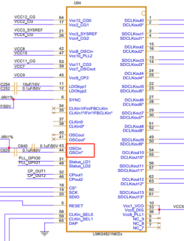
Synchronization scheme (status): The 125M input is provided by another module on each board, and the modules are connected through switches to ensure that the 125M reference clock input is from the same source and synchronized; Our solution for synchronization between multiple boards is to send a pulse through the sync pin to achieve synchronization. The specific method is to send a trigger signal to both boards simultaneously through an external signal source. When this signal is detected by the FPGA, a enable is raised. During the effective period of the enable, when the 1pps signal sent by the 125M clock module is detected, the two signals are in phase with each other in the logic, and the new signal after it is used as the synchronization event of 04828 in the multiple boards (the accuracy of the synchronization event cannot reach ps level)
Our main concern now is to know if our current solution is feasible. If so, at what stage should the sync signal be given and how should the registers be configured?
I have now tried and found that when I give the sync signal, I observed the sysref signal output by 04828 on two boards through an oscilloscope and found that there was no action. Therefore, I am not sure if our solution is not feasible or if there is a problem during the configuration process. I would like to ask for guidance on this matter.

  • Hi Jeno,

    Would you care to share your configuration file?

    And just so I am clear, you have two separate LMK04828 boards whose outputs you want synchronized? Or you are trying to synchronize the outputs from one LMK04828?

    In the case of the former, is it possible for you to change your SYNC input from the SYNC pin to CLKin0? See this link for more details.

    Thanks,

    Michael

  • Hello,

    The following is the register configuration file without debugging the synchronization of multiple boards.

    R0 (INIT)	0x000090
    R0	0x000010
    R2	0x000200
    R3	0x000306
    R4	0x0004D0
    R5	0x00055B
    R6	0x000600
    R12	0x000C51
    R13	0x000D04
    R256	0x010014
    R257	0x010155
    R258	0x010255
    R259	0x010301
    R260	0x010422
    R261	0x010500
    R262	0x010670
    R263	0x010766
    R264	0x010814
    R265	0x010955
    R266	0x010A55
    R267	0x010B01
    R268	0x010C22
    R269	0x010D00
    R270	0x010E70
    R271	0x010F66
    R272	0x011008
    R273	0x011155
    R274	0x011255
    R275	0x011301
    R276	0x011422
    R277	0x011500
    R278	0x011670
    R279	0x011760
    R280	0x011818
    R281	0x011955
    R282	0x011A55
    R283	0x011B01
    R284	0x011C22
    R285	0x011D00
    R286	0x011E70
    R287	0x011F10
    R288	0x012008
    R289	0x012155
    R290	0x012255
    R291	0x012301
    R292	0x012422
    R293	0x012500
    R294	0x012670
    R295	0x012710
    R296	0x012808
    R297	0x012955
    R298	0x012A55
    R299	0x012B01
    R300	0x012C22
    R301	0x012D00
    R302	0x012E70
    R303	0x012F60
    R304	0x013006
    R305	0x013155
    R306	0x013255
    R307	0x013301
    R308	0x013422
    R309	0x013500
    R310	0x013671
    R311	0x013701
    R312	0x013800
    R313	0x013903
    R314	0x013A03
    R315	0x013B00
    R316	0x013C00
    R317	0x013D08
    R318	0x013E01
    R319	0x013F00
    R320	0x014081
    R321	0x014100
    R322	0x014200
    R323	0x014311
    R324	0x0144FF
    R325	0x01457F
    R326	0x014608
    R327	0x01471F
    R328	0x014802
    R329	0x014942
    R330	0x014A02
    R331	0x014B16
    R332	0x014C00
    R333	0x014D00
    R334	0x014EC0
    R335	0x014F7F
    R336	0x015003
    R337	0x015102
    R338	0x015200
    R339	0x015300
    R340	0x015478
    R341	0x015500
    R342	0x015678
    R343	0x015700
    R344	0x015896
    R345	0x015900
    R346	0x015A0A
    R347	0x015BD4
    R348	0x015C20
    R349	0x015D00
    R350	0x015E00
    R351	0x015F0B
    R352	0x016000
    R353	0x016104
    R354	0x016224
    R355	0x016300
    R356	0x016400
    R357	0x01650C
    R369	0x0171AA
    R370	0x017202
    R380	0x017C15
    R381	0x017D33
    R358	0x016600
    R359	0x016700
    R360	0x016828
    R361	0x016959
    R362	0x016A20
    R363	0x016B00
    R364	0x016C00
    R365	0x016D00
    R366	0x016E13
    R371	0x017300
    R386	0x018200
    R387	0x018300
    R388	0x018400
    R389	0x018500
    R392	0x018800
    R393	0x018900
    R394	0x018A00
    R395	0x018B00
    R8189	0x1FFD00
    R8190	0x1FFE00
    R8191	0x1FFF53
    

    The following is the register configuration file for debugging synchronization of multiple boards.

    lmk04828_zdm_singleloop(1).tcs

    Thanks!

  • Hi Jeno,

    I took a look through your configuration file, and I found that your boards are in single loop zero delay mode. This is crucial to your synchronization arrangement, because it allows you to be able to send the SYNC pulses to the boards without the constraint on the order of ps. The looped back output is input to the PLL2 N divider, resulting in phase lock between the OSCin signal and CLKout8. 

    What needs to happen from here is that a SYNC pulse needs to be issued to the boards, but ultimately the timing is not as crucial. Any SYNC pulse, regardless of the cycle it arrives in, will result in all of the outputs sharing phase alignment. Given that there is already an output with a deterministic relationship to the input frequency, all other outputs will be aligned to that output, resulting in a deterministic phase relationship between the input and all output clocks. 

    The main thing I had to change was the setting of the SYNC_DISx bits. Setting these high prevents the corresponding outputs from being synchronized by a SYNC event. Using this device, I was able to see outputs (including the SYSREF outputs, but only after the SYNC event).

    I have attached the file I used for debug for convenience.

     lmk04828_zdmsl_update.tcs

    Thanks,

    Michael