This thread has been locked.

If you have a related question, please click the "Ask a related question" button in the top right corner. The newly created question will be automatically linked to this question.

LMK04828: Clarification on CLKin behavior in High-Z mode with 100-ohm termination compared to external fail-safe biasing (LMK04828)

Part Number: LMK04828

Hello TI Support Team,

I am designing a clock tree using the LMK04828 and have a question regarding the CLKin input requirements (used for JESD204B SYSREF) when the driving source is temporarily disabled.

[System Setup]

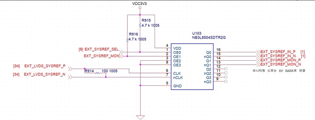
I am driving the LMK04828 CLKin0 port with an external LVDS fanout buffer (NB3L8504S).

The signal is DC-coupled with a 100-ohm differential termination resistor placed close to the LMK04828 input pins.

The buffer has an Output Enable (OE) pin. When the OE pin is pulled LOW, the LVDS outputs go into a High-Impedance (High-Z) state.

[My Inquiry]

In the LMK04828 datasheet (Section 10.7 Do's and Don'ts), it states: "Unused Clock Inputs: unused clock inputs can be left floating."

However, my CLKin is not physically "unused" or completely unconnected; it is dynamically turned off (High-Z) via the buffer's OE pin while still connected to traces and the 100-ohm termination. In this High-Z state, the differential voltage ($V_{ID}$) across the 100-ohm resistor essentially becomes 0V.

Could you please clarify the following based on the datasheet specifications?

Risk of False Triggering (Chattering): Since V_ID = 0V falls into the threshold region of the receiver and violates the minimum |V_ID| specification, will leaving the buffer in High-Z cause chattering or false SYSREF triggering due to ambient noise picked up by the traces?

Fail-Safe Biasing Requirement: To prevent any metastable state, is it officially recommended to add an external fail-safe bias network (e.g., 1k-ohm pull-down on the P-line to GND, and 1k-ohm pull-up on the N-line to 3.3V) to force a stable Logic LOW state when the driver is High-Z?

Logic LOW vs Logic HIGH: If external biasing is necessary, does it strictly need to be biased to Logic LOW for proper JESD204B SYSREF operation (to prepare for a clean rising edge), or would biasing it to Logic HIGH also be acceptable?

I would appreciate your detailed technical explanation. Thank you!

  • Hi There,

    CLKin0 pins has internal bias but there is no offset voltage between them. So if the input pins are physically left floating, chattering may happen. When your LVDS driver output is Hi-z, CLKin0 is still connected to the 100Ω resistor and the output of the LVDS driver. With this configuration, it is hard to tell if chattering would happen. In fact, even if your LVDS driver is enabled but the output is static (logic 0 or logic 1), the situation is same as if the LVDS driver is Hi-Z because the AC-coupling capacitors have blocked the DC from the driver. 

    Suggest change CLKin0 type to MOS, there will be an offset voltage between the pins to prevent chattering.

  • Hi there,

    Thank you for the clear explanation regarding the MOS buffer mode.

    I have a follow-up question regarding the AC-coupling capacitors you mentioned and our specific use case.

    The signal we are feeding into CLKin0 is a JESD204B SYSREF. Specifically, we are using an LVDS fanout buffer (NB3L8504S) to drive this signal. We will control the buffer's OE (Output Enable) pin to send discrete bursts of exactly 2 pulses, after which the OE pin will be disabled, immediately putting the driver output into a High-Z state.

    Because this is a pulsed signal with long idle periods (unlike a continuous high-frequency clock), using AC-coupling capacitors could cause DC wander or block the SYSREF pulses entirely. Therefore, we must use DC coupling (a direct connection without AC capacitors) between the NB3L8504S outputs and the CLKin0 pins.

    Could you please confirm if my following understanding is correct?

    In this DC-coupled configuration, is it sufficient to just change the CLKin0 type to 'MOS' via SPI registers to prevent any chattering when the NB3L8504S driver enters the Hi-Z state after sending the 2 pulses? Or is there any other hardware/software consideration we need to be aware of?

    Thanks again for your great support.

  • Hello,

    Because this is a pulsed signal with long idle periods (unlike a continuous high-frequency clock), using AC-coupling capacitors could cause DC wander or block the SYSREF pulses entirely. Therefore, we must use DC coupling (a direct connection without AC capacitors) between the NB3L8504S outputs and the CLKin0 pins.

    This is correct. Furthermore, the MOS mode input amplifier has larger hysteresis levels at the MOSFET input than the Bipolar mode input circuit, making it optimized for DC-coupled applications. Setting CLKin0 type to MOS is sufficient to accommodate this.

    Thanks,

    Michael

  • As previously discussed in a related thread (see second attachment), we are driving CLKin0 with an LVDS fanout buffer (NB3L8504S). To meet JESD204B requirements, we send discrete bursts of exactly 2 pulses by toggling the buffer's Output Enable (OE) pin. When idle, the driver enters a High-Z state.


    MOS Mode Confirmation: The previous advice suggested using MOS mode for CLKin0 to utilize higher hysteresis and prevent chattering during the High-Z state.

    In my current TICS Pro configuration I have set CLKin0 to 4 MHz and intended to use it as the reference for SYSREF MUX. However, the PLL1 R Dividers for the CLKin0 path are currently greyed out (inactive) and I am unable to configure the LOS (Loss of Signal) settings for CLKin0 in the "PLL1 Reference Input Select" block.

  • Hello,

    LOS functionality only applies to the PLL input path. If the CLKin0 signal is routed to the SYSREF Mux, LOS functionality cannot be applied to that input.

    Thanks,

    Michael

  • Subject: Clarification on SYSREF Mux Input Type (MOS), Coupling, and Independent Port Configuration for LMK04828

    Hello Michael,

    Thank you for your previous detailed explanations. I would like to finalize our design based on your advice and have a few last questions to ensure everything is correct.

    Our ultimate goal is to have the LMK04828 reliably recognize a LOW state when the NB3L8504S output is in High-Impedance (Hi-Z), especially since we are using 2-pulse bursts for SYSREF.

    1. Input Mode Selection: As you suggested, the LOS (Loss of Signal) function is only for the PLL path and not available for the SYSREF Mux path. Therefore, is it correct that simply setting the CLKin0_TYPE to MOS mode is the best and only necessary configuration to ensure a stable state and prevent chattering during the Hi-Z period?

    2. Coupling (AC vs. DC): To ensure that the LMK04828 correctly recognizes the High/Hi-Z transitions from the NB3L8504S, should we use DC coupling? Since we need the input to stay at a specific logic level (Low) during the Hi-Z state of the driver, my understanding is that DC coupling is required to maintain that reference. Could you confirm if DC coupling is recommended for this MOS mode setup?

    3. Independent Port Configuration (CLKin0 vs. CLKin1): In our design, we are planning to use different input types for each port. Is it acceptable to configure CLKin0 as MOS mode while simultaneously using CLKin1 in Bipolar mode? I want to confirm that these ports can operate independently with different input type settings without any interference.

    4. Final Verification: In summary, if we use DC coupling, set the SYSREF Mux input (CLKin0) to MOS mode, and potentially use CLKin1 as Bipolar, will the LMK04828 work reliably (staying LOW during Hi-Z and correctly capturing the 2-pulse bursts) without any additional external fail-safe biasing resistors?

    I look forward to your final confirmation. Best regards.

  • Hello,

    1. Input Mode Selection: As you suggested, the LOS (Loss of Signal) function is only for the PLL path and not available for the SYSREF Mux path. Therefore, is it correct that simply setting the CLKin0_TYPE to MOS mode is the best and only necessary configuration to ensure a stable state and prevent chattering during the Hi-Z period?

    Yes, this is sufficient. 

    2. Coupling (AC vs. DC): To ensure that the LMK04828 correctly recognizes the High/Hi-Z transitions from the NB3L8504S, should we use DC coupling? Since we need the input to stay at a specific logic level (Low) during the Hi-Z state of the driver, my understanding is that DC coupling is required to maintain that reference. Could you confirm if DC coupling is recommended for this MOS mode setup?

    Yes, DC coupling is recommended for this MOS mode setup.

    3. Independent Port Configuration (CLKin0 vs. CLKin1): In our design, we are planning to use different input types for each port. Is it acceptable to configure CLKin0 as MOS mode while simultaneously using CLKin1 in Bipolar mode? I want to confirm that these ports can operate independently with different input type settings without any interference.

    Yes, this should be fine.

    4. Final Verification: In summary, if we use DC coupling, set the SYSREF Mux input (CLKin0) to MOS mode, and potentially use CLKin1 as Bipolar, will the LMK04828 work reliably (staying LOW during Hi-Z and correctly capturing the 2-pulse bursts) without any additional external fail-safe biasing resistors?

    That is correct.

    Thanks,

    Michael