LMK05028: DPLL Reference clock input

Part Number: LMK05028
Other Parts Discussed in Thread: LMK00804B

image.png

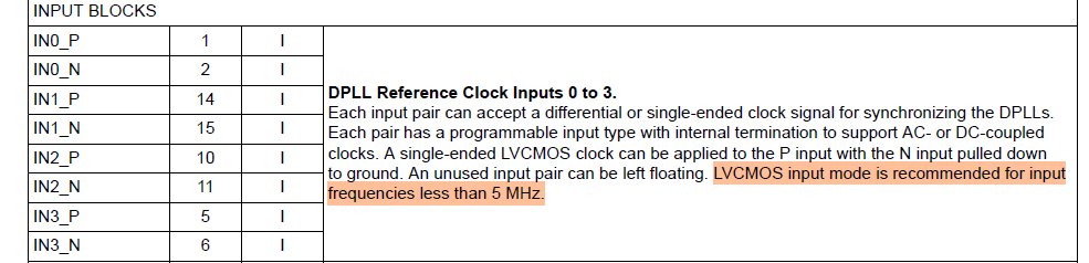
We want to connect to VSC8512 PHY recoverd clock(125MHz) to PLL(LMK05028) Input which is LVCMOS, But according to the snippet attached LMK05028 Datasheet is saying that LVCMOS can take only less than 5MHz. So please tell us this will work or not? If it works do we need any specific termination for it?


Thanks & Regards,

J Shashikanth Reddy


  • Hi, 

    I'll take a look into this to see if there's any limitation with using a 125MHz LVCMOS input here. I should be able to get back to you with some feedback tomorrow. 

  • Hi, 

    The note that "LVCMOS input mode is recommended for input frequencies less than 5MHz" is just indicating that for reference frequencies < 5MHz it's recommended to use the LVCMOS input type instead of a differential input. You can refer to the reference input characteristics provided in the electrical characteristics table (also pasted below). LMK05028 can support a 125MHz LVCMOS input without any issues. Let me know if you have any other questions on this. 

  • Hi Lewis,

    Thank you for your quick response.

    we have one more query that Recovered clock we are mapping on PLL input level is 2.5V and PLL  Vin Supply Voltage is 3.3V.  will it work fine ?  as we can not level translate.

    • Here iam attaching PLL Part schematics. Please review once and provide your feedback.Qbit PLL DSN.pdf
  • Hi Shashikanth, 

    That should be fine, the LMK05028 reference input is rated to work with a minimum single-ended swing of 1V. I also reviewed the schematic and it looks good, no other feedback on my end. 

  • Thanks Lewis for your feedback. it helped a lot for us.

  • Hi Lewis,

    Can we connect 1.8V PPS differential output from FPGA to LMK00804BPW Buffer .will it work?

  • Hello Lewis, sorry for back to back questions.

    Here in LMK05028 PLL, we are giving 1.8V Supply to GPIO Pins and VDDDIG Supply is connected to 3.3V .is this ok or we need to connect GPIO pins with respect to VDDDIG?   Please confirm.

    Also PLL Outputs, one connected to FPGA GTH(Transceiver) Bank and one more connected to HP Bank(1.8V) .Will it work ?

    Thanks & Regards,

    J Shashikanth Reddy

  • Hi Shashikanth, 

    For LMK00804B it should be ok to use a differential 1.8V 1pps as the input, but you will have to double check that you're not violating the differential input swing max or common mode requirements. Is each leg of the differential pair swinging from 0V to 1.8V? Or is this some other type of signaling format?

    For LMK05028, the GPIO are compatible with 1.8V logic since anything above 1.2V is considered a logic high, so I think this should be ok. Can you clarify on the requirements for the clock outputs? Since the outputs are AC-coupled in your schematic I assume that the receiver will have its own termination / biasing scheme to set the correct common mode voltage. Do the different receivers have different amplitude requirements for the clocks? 

  • Hi Lewis, Thanks for the reply,

    Our PLL Output is AC Coupled and it is going to different outputs, 2 Outputs are going to GTH Ref Clock and One clock output to LVDS2V5 AND one more Output going to LVDS1V8. 

    For LVDS1V8 Specification Table attached for reference. and No Biasing  & termination provided Internally.

    For GTH we have internal termination and VCIM is 800mv . 

    Are we in trouble with any of the PLL Outputs. if yes how can we rectified?

    Thanks & Regards,

    J Shashikanth Reddy

  • Hi Shashikanth, 

    When you say that the LVDS 1.8V clock doesn't have an internal input termination, is there still a 100 Ohm differential termination included externally? The AC-LVDS driver from LMK05028 expects a 100 Ohm termination in order to generate the correct signal amplitude. Assuming there is an external 100 Ohm termination then LMK05028 should be able to meet the amplitude requirements. You'll still need some kind of bias to set the common mode voltage, either externally or internally on the receiver.