


Hi,
We are planning to use CDCM7005 in our design.
Design requirements:
#################
1. 5 Clock outputs (Fout = 102.4MHz) to drive 4 ADCs and External reference.
2. We are planning to use ADC AD9467 (Analog devices). The ADC supports 75dBc SNR (Input 70+/- 10MHz / 1.5MHz to 30MHz , Sampled at 102.4MHz) .
3. CDCM7005 should lock to an External OCXO (Reference Clock) with sine wave 10MHz (Phase noise -130dBc/Hz @10KHz and higher) which is yet to be selected.
Query:
#####
1. Will the CDCM7005 will provide sufficient low jitter clock to meet the SNR spec of the ADC (RMS clcok jitter should be less than approximately 350fS. Correct me if I am wrong).
2. Since the OCXO is yet to be selected. How to derive the jitter requirement of the OCXO from the design requirement for the CDCM7005 (RMS Jitter < 350fS)
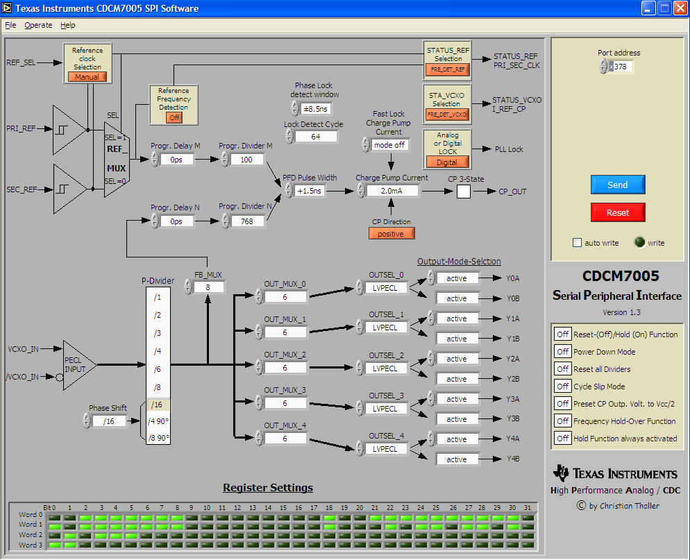
3. Is there any frequency planner available for CDCM7005 (Such as one available for CDCM61001 http://e2e.ti.com/support/clocks/m/videos__files/576535.aspx ). I want to derive the VCXO frequency for the 10MHz reference and 102.4MHz output with the possible M, N & P divider values.
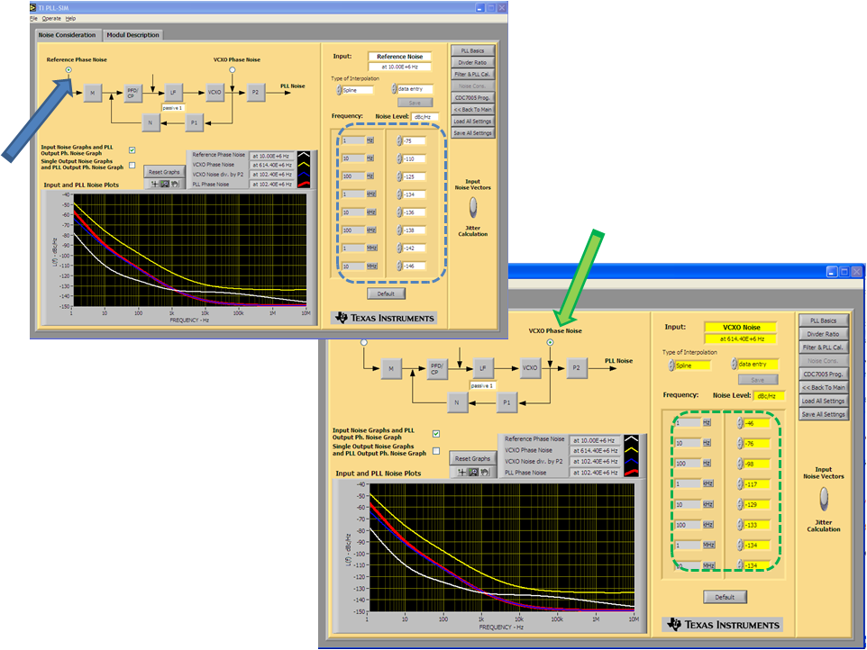
4. We are planning to use the VCXO (http://www.silabs.com/Support%20Documents/TechnicalDocs/si570.pdf). Please let me know how can I estimate the phase noise of CDCM7005 output from VCXO and OCXO phase noise information. I refereed the http://e2e.ti.com/support/clocks/f/48/t/153019.aspx. But unable to find out where to give the phase noise informations of the VCXO and OCXO to get the resultant phase noise of the CDCM7005.
Regards,
Kiruba
