Because of the holidays, TI E2E™ design support forum responses will be delayed from Dec. 25 through Jan. 2. Thank you for your patience.

This thread has been locked.

If you have a related question, please click the "Ask a related question" button in the top right corner. The newly created question will be automatically linked to this question.

Problem about LMK02000

Other Parts Discussed in Thread: LMK02000, LMK03000, SN65LVDS32, CODELOADER, LMK04100, LMK04000, LMK04803, LMK04033, LMK03806

Now, I use LMK02000 chip and have met some problem. when I only enable CLKOUT0, the output of the CLKOUT0 is right and the divider and delay time about the CLKOUT0 is correct. but when I enable some other clock-x output.,all the anable outputs are not work and some output signals are DC signal with 1.6V, and some is about 0V,what reasons can cause this problem? 

There is another priblem, when LMK02000 is going to lock the reference clock, the frequency of VCXO deviates from  the reference clock suddenly and the deviation of the frequency is a little big, that is why? what reason maybe cause the frequency of VCXO changing quickly whe LMK02000 is close to lock the reference clock?

I also find a problem about datasheet of the LMK02000, The chip of LMK02000 used is the national semiconductor corpotation, I find the datasheet released in 2006 and datasheet released have some differences about the control rigister-R0,R14,R15,and this three registers are very improtant for using the chip. how to fiind the differences of LMK02000 chip about the two kind of datasheets?

  • Hi Jie,

    Pls note that for LVPECL outputs (CLKout3 to 7), they need pull down bias resistors. Pls refer to LMK03000 datasheet, section 3.7 for details.

    Did you mean the VCXO freq chagne periodically? Configure PLL_MUX to "Digital LD Active High" and check what is the status of the LD pin. If it is locked, you should see a stable logic High.

    I have a 2007 National version datasheet and the latest TI version datasheet, I don't see there is difference on register R0, 14, and 15. Would you point out the difference?

  • Hi Noel,

    when the LMK02000 chip is closed to lock the external VCXO, the VCXO frequency change sundenly, and this process appear periodically.  I have ckecked the LD pin and this pin always is low level during the processing, and I hvave set the " PLL_MUX" to "Digital LD Active High" .

    In order to  check wheather the data  writed is correct or not, I have configured "PLL_MUX" to "logic high,logic low, N Divider Output/2 and R Divider Output/2" and the output of  LD pin are all correct.

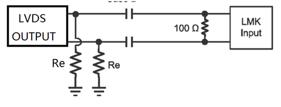
    The Following is the input of OSCin and Fin, Does the input circut has some problem? the emtier risistors (Re) is 240 Ohms in the picture

    The attachment is datasheet of LMK released  by national semoconductor companny in 2006, and there are some differences between datasheet in 2006 and datesheet current.

    0878.LMK02000-2006.pdf

  • Hi Jie,

    When you see logic LOW when PLL_MUX is configured as LD, that means the VCXO is never locked.

    Pls note that AC-couple is required for both OSCin and Fin pins. Recommended connection for LVDS and LVPECL source are as follows.

    The 2006 datasheet you have is not the final released version. Pls use the latest TI version datasheet.

  • what do this sentence mean " When you see logic LOW when PLL_MUX is configured as LD,  that means the VCXO is never locked."? I  configure  the PLL_MUX to " logic low. logic high, and R or N  Divider Output/2" for testing whether the writed data is correct. The PLL_MUX is configured to "Digital Lock Detect (Active High)" when the LMK02000 chip work. Is the VCXO not locked the external refence clock when the PLL_MUX is configured to "Digital Lock Detect  (Active High)"?

    I use the infomation about the LVPECL output and all the LVPECL output can work right, but all the LVDS output can not work and the output signal are DC signal of 1.6V.

  • Hi Noel,

    I have another quetion about the LVDS output, Do the LVDS outputs can work when they connect nothing or  a 100 Ohms resistor was placed between positive  terminal  and negetive terminal? Can you give me some useful circut when the LVDS outputs connect with SN65LVDS32 chip?

    Thank you!

  • Hi Jie,

    When you put PLL_MUX to "Digital lock detect active high", a High output on the LD pin means it is locked. As you saw a Low output, that means it is unlocked. First of all, make sure both OSCin and Fin pins are connected properly, remember AC-couple is required. Secondly, make sure the loop filter is properly design. Lastly, you should program the device properly. We recommend use CodeLoader to generate the register settings.

    To interface LVDS clock output with SN65LVDS32, we recommend AC-couple. It is because SN65LVDS32 has internal input bias voltage.

  • Hi Noel,

    How much frequency difference will make the LMK02000 chip set lock label(logic high)? Now, I have compared the refence clock and VCXO frequency, and the frequency difference between both is very small and the frequency error is less than 5E10-11 for 12hours, but the LMK02000 chip do not set the lock label. what kind of reason can prevent it set the lock label?

    I always use the  CodeLoader  and clock design tool soft during testing the circut.

    Thank you!

  • Hi Noel,

     There is another problem about clock, there are two different frequecy of output? the frequency of one output is 10MHz and another is 100MHz, and fhe frequency of the reference and external VCXO are 10MHz, which chip can be used to realized the design?

    I have used the clock design tool and it provides many clock clear chips,such as  LMK04100, LMK04000 LMK04033 and LMK04803. which chip the best choice for this design and the 100MHz clock output need smalller noise tthan the 10MHz in this design. what is the main difference among the chip provided by the clock design tool?

    thank you !

  • Hi Jie,

    I'll have to look into details of your desgin. Would you provide the CodeLoader configuration file (.mac file) and the schematic?

  • Hi Jie,

    If your application is jitter cleaning, you need LMK02xxx or LMK04xxx. If it is a clock generation application, LMK03806 is recommended.

    LMK041xx is low cost and good for most of the applications.LMK048xx and LMK040xx has better performance but LMK048xx offer more output and configurable LVDS/LVCMOS/LVPECL output. LMK040xx has fixed the number of differential and single-ended output.


  • Hi Noel,

    The attachment is the CodeLoader configuration file and schematic about LMK02000 part. During progamming the LMK0200 chip, I firstly reset the chip by set the reset bit in R0 controling register, and then set other controling register in order.

    3660.LMK02000.rar


  • Hi Jie,

    You have a very complicated matching network in Fin and OSCin. What is the output type (LVCMOS or LVPECL) of the reference source and the VCXO?

    In addition, your loop filter is not corret, R46 is never open. Could you send me the specification of the VCXO? I need this information to calculate the correct loop filter value.

    Suggestion on the output interface to LVDS32 as follows:

  • hi Noel,

      this schematic is the first version and i want to test the performance of LMK02000 at different input situation, so the match net is complicated, the type of  the reference source and the VCXO is sinusoid, but I use the TLC3501 and sn65lvds32 chip, and the input type of the LMK02000 on Fin and OSin are LVDS.

    the VCXO used is JTM5000 series of JUSTIMING TECHNOLOGY  and the web site is http://www.justiming.com.

    the output circut  of LVDS I have used and the output is also a DC signal of 1.6V.

    Is the set of controling information correct?

    in addition, R45 is not open and is used as the R2 in the clock design tool.

  • Hi Jie,

    You are actually using an OCXO instead of a VCXO. What are the supply voltage and tuning range of the OCXO?

    If the OCXO supply voltage is greater than 3.3V, you may not be able to have it locked using LMK devices at the max output tuning voltage of LMK devices are less than 3.3V.

    Usually, the tuning range of OCXO is very small, around 1 to 2ppm. If the input reference source has a frequency tolerance greater than 2ppm, you will also not able to get it locked.

    You got very accurate output frequency simply because you are using an OCXO, no matter whether it is locked or not.

    The LMK device might has damaged by DC coupling to LVDS32. Use a new LMK2000, make sure it is AC couple to LVDS32 before you power up the device.

  • Hi Noel,

      the turning voltage range is less than 5V and I have measured that the turning voltage is about 2.5V when the frequency error between the reference and OCXO is every little.

    I have tested this circut for several days and I find that the VCXO can lock reference and LMK02000 also set the lock label.but sometimes the ship do not set the lock label and the frequency error is also every little . I have  read   the LMK04800 datasheet and speacial about the "DIGITALLOCKDETECT" part. what I understand about this part is that when the frequrcy between reference and VCXO is every little and  the phase error is not less than ε, the chip will not set lock label. It is the same to LMK02000.

     I also read "SerialMICROWIRETimingDiagram"  fo LMK04800, there is "ADVANCEDMICROWIRETIMINGDIAGRAMS" for LMK0480x chip. Does the LMK02000 also exist the "ADVANCEDMICROWIRETIMINGDIAGRAMS" ?

    If I use the OCXO, Do the LMK02000 chip can lock the extern reference?

    I think if the statbility of  the reference  is good  enough and the frequency of the refence is in the range of the OCXO, the OXCO also can lock the refence. Do you think so?