This thread has been locked.

If you have a related question, please click the "Ask a related question" button in the top right corner. The newly created question will be automatically linked to this question.

CDCM6208 output issue

Other Parts Discussed in Thread: CDCM6208

Hi All,

We are unable to configure the device in I2C mode as it is not acknowledging. We confirmed it through probing on the clock and data pins. Even the default outputs are absent. we could able to see some DC shifts on the CLK output pins (1.8V DC on CLK_P and 3.3V on CLK_N pins). We tried to program it from FPGAs (ARTIX  and SPARTAN).

Even the PIN mode is not working for us. Same is the case with outputs in PIN Mode.


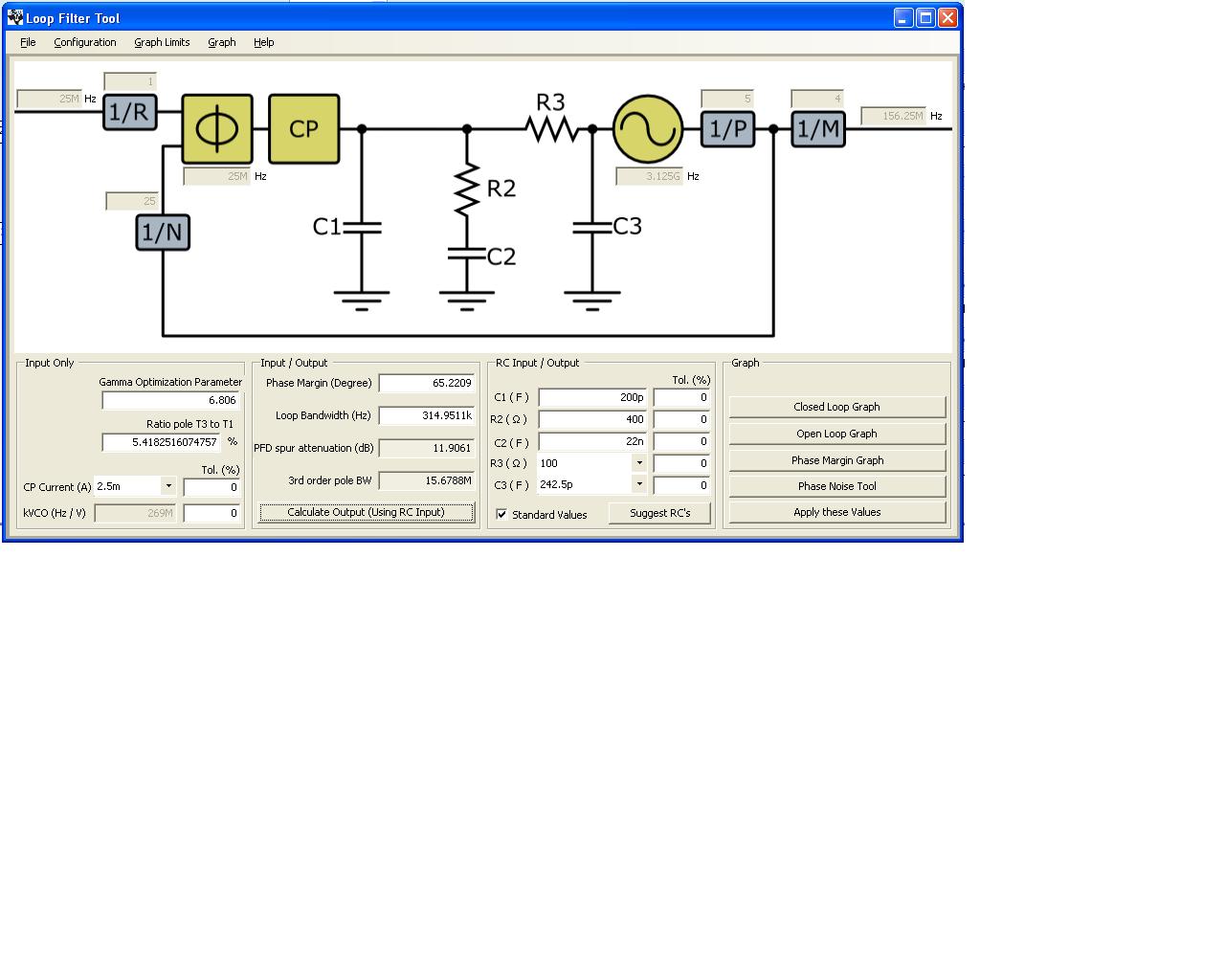
Please find the attached schematic file and clock synthesizer loopfilter and frequency planner images7658.TCC_SCH.pdf
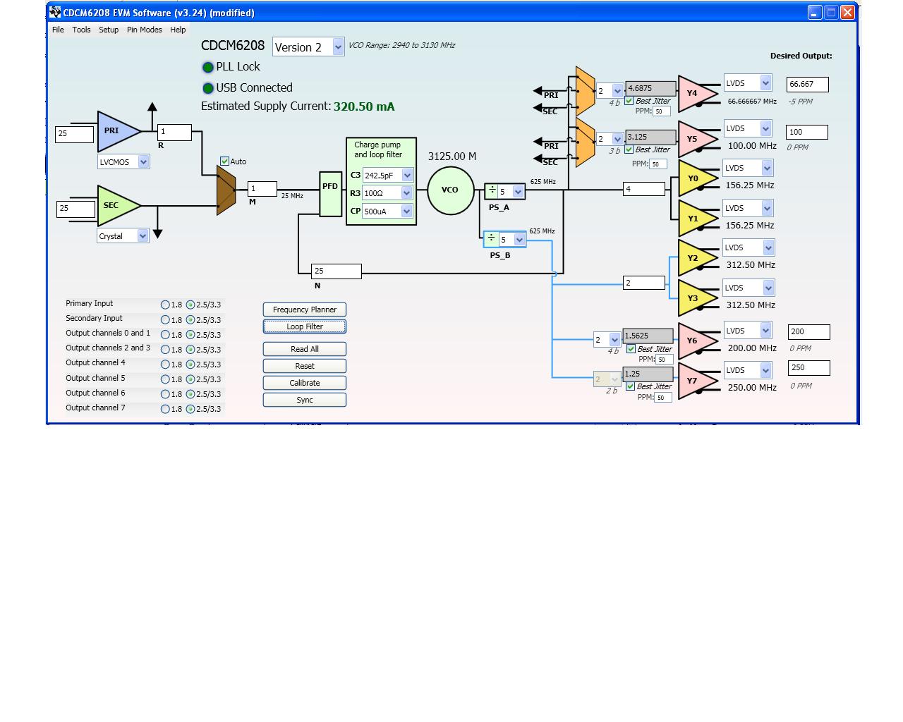
Thanks and regards,

Manjunath

  • Hello Manjunath,

    let me rephrase the issue to make sure I do understand it.

    - You have a an FPGA host connected to a single CDCM6208

    - You are sure that your host is working properly as an I2C host by probing SDA/SCL

    - when CDCM6208 is configured in I2C mode is not responding ACK, i.e. I2C communication failed

    - when CDCM6208 is configured in pin-mode, output frequencies are not as expected. i.e pin-mode is no working


    Some things to quickly check

    - are you using CDCM6208 version 2 as the capture shows, VCO ferq is differnt?

    - the CP current is inconsistent between the two figures (500u or 2.5mA), which one is used?

    - is SI_MODE[1:0] set to "01" for I2C mode, and left open or set to "10" for pin mode?

    According to the schematic attached, CLK_SYN_MODE[1:0] = "00". this actually sets the SPI mode instead

    This anyway has to be fixed before being able to communicate using I2C or set pin-mode

    - is the AD[1:0] set to the address used by the host for the I2C mode?

    According to the schematic attached, CLK_SYN_AD[1:0] = "00".


    Please do those simple checks first and let me know the results.

    Can you elaborate more on this statement:

    "we could able to see some DC shifts on the CLK output pins (1.8V DC on CLK_P and 3.3V on CLK_N pins)"

    Ahmed