Part Number: LMX2571
Other Parts Discussed in Thread: PLLATINUMSIM-SW
hi,
Now I am trying to design a 1W transmitter for our customer with your smart IC—LMX2571; 49channels with carrier range from 72.08MHz—72.98MHz, the carrier pitch is 20KHz;
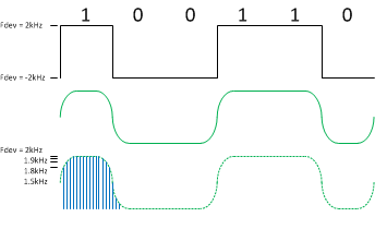
We take the advantage of the Direct Digital FSK Modulation of your Smart IC, FD=+1.8KHz ----1
FD=-1.8KHz ----0
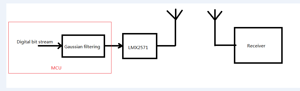
Here is the blockdiagram, and the some configuration of Synthesizer Duplex Mode;
cid:image001.png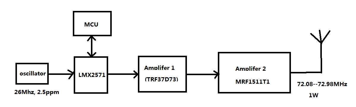
cid:image002.png

The circuit of LMX2571 is as Picture1 in attached picture(open it with paint), any problem or suggestions?
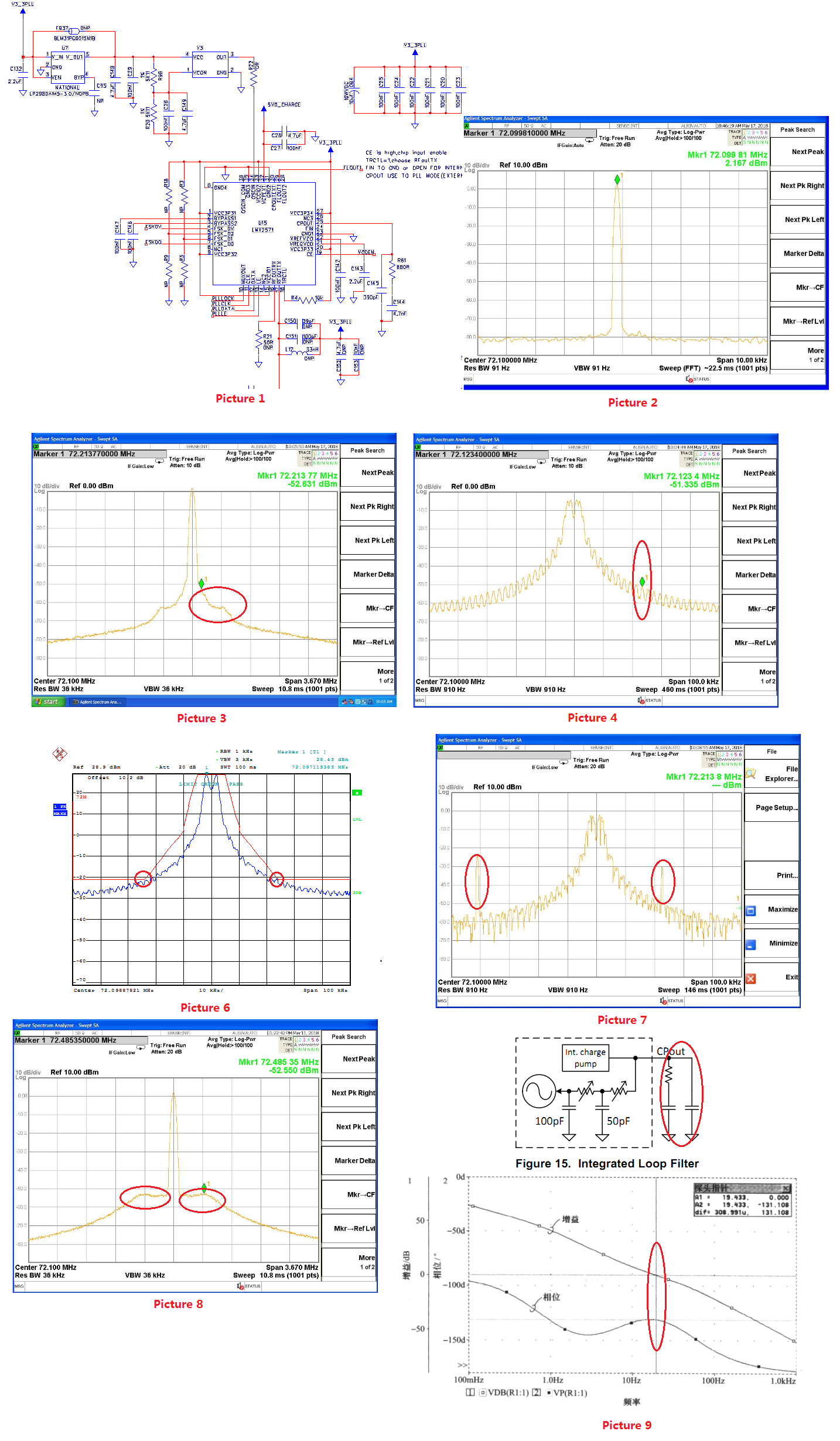
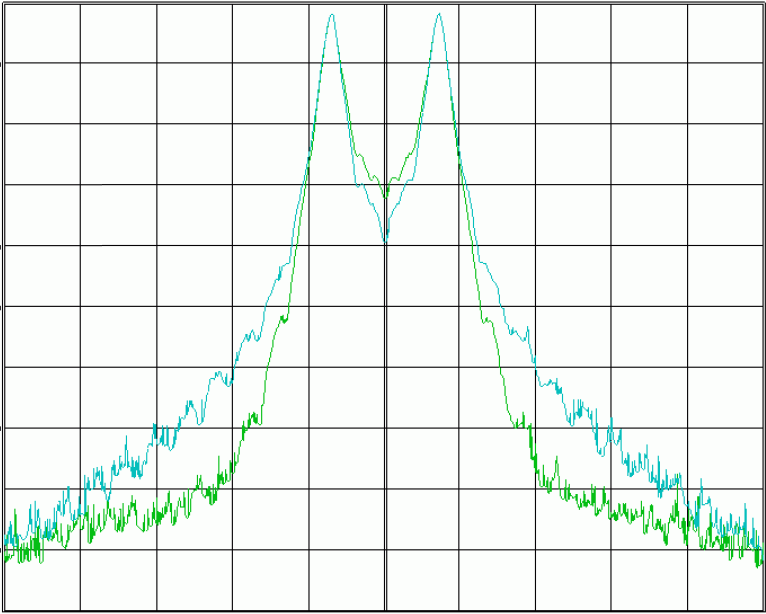
When we disable the FSK, with setting FSK_EN_F1, FSK_EN_F2 to 0, the output frequency spectrum(between Amplifier 2 and Antenna) is very good(Picture2 in attachments, span is just 10k), so when LMX2571 close its FSK function, the output frequency spectrum is very good;
When we enable the FSK, with setting FSK_EN_F1 =1, FSK_EN_F2= 1( and setting LF_R3/R4_F2/F1=1, CP_IUP/IDN=1;) the output frequency spectrum(between Amplifier 2 and Antenna) is as picture3,4(span is 3.67MhZ and 100k), much worse than picture2; Furthermore it can’t pass conductive bandside test of FCC part90, as picture6,
So we have to optimize bandside , with setting LF_R3/R4_F2/F1=0, CP_IUP/IDN=16, (and with setting FSK_EN_F1 =1, FSK_EN_F2= 1), now the bandside just improve a little(2DB margin), but phase noise deteriorated(picture8), can’t find a balance..
And we did try to use some more stable oscillator, unluckly no any improve;
From above description, we can get that how much/greatly The FSK modulation affect/effect the bandside noise;
We guess that maybe revising some FSK modulation parameters can fix this problem, --getting both phase noise and bandside well; but we don’t know how to do it;
So could you do me a favor to offer some suggestions about revising some FSK modulation parameters to fix this problem??
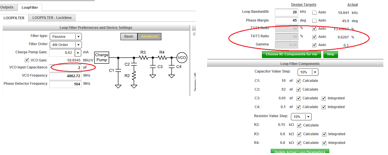
By the way, when we set LF_R3/R4_F2/F1=1, CP_IUP/IDN=1; there are some spur in the frequency spectrum(Picture7), we guess the parameters of LPF was not the best,
as we know, the best situation of PLL is the phase margin at the point of loop bandwidth is about 40-50 degree( as picture9), but how to estimate the value of resister and capacitor in LPF(figure15 in picture9) to get the best phase margin at the right frequency(loop bandwidth)? Do you have any suggestions? Or any paperwork? Or is there any software tool for it ?