This thread has been locked.

If you have a related question, please click the "Ask a related question" button in the top right corner. The newly created question will be automatically linked to this question.

LMK04828BEVM: LMK04828BEVM DCLK0 output levels to drive DAC3484EVM CLKIN on J9 (i.e. to the CDCE62005 External Clock input)

Part Number: LMK04828BEVM
Other Parts Discussed in Thread: CDCE62005, DAC3484EVM, DAC3484, CDCM7005

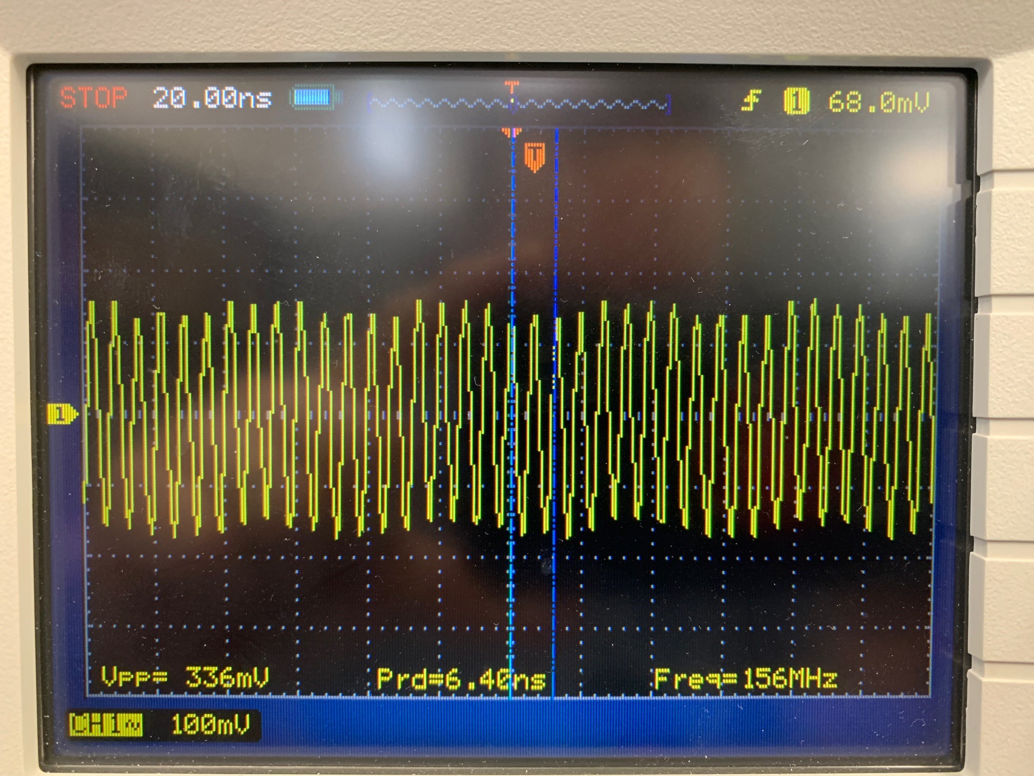
I'm driving out 1 1Vpp 153.6MHz LVPECL20 +/- signal from CLKout0/CLKout0* and connected to a ADC-WB-BB balun that connects to the J9 CLKIN input of the DAC3484EVM.  The signal gets attentuated to a 24mVpp signal riding on a 200mV DC bias to the on-board CDCE62005 PRI REF+ input.  I don't believe that this external clock is making it through the clock chip to provide a clock output back to the FPGA.  The output is 2.72VDC on both FPGA_CLKOUTP and FPGA_CLKOUTN.  I've attachecd the DAC3484EVM register setup file. 

DAC3484EVM_setup_registers.txt
   x00	   x089C
   x01	   x050E
   x02	   xF002
   x03	   xF000
   x04	   x4068
   x05	   x3B60
   x06	   x2500
   x07	   xFFFF
   x08	   x0000
   x09	   x8000
   x0A	   x0000
   x0B	   x0000
   x0C	   x0400
   x0D	   x0400
   x0E	   x0400
   x0F	   x0400
   x10	   x0000
   x11	   x0000
   x12	   x0000
   x13	   x0000
   x14	   x0000
   x15	   x0000
   x16	   x0000
   x17	   x0000
   x18	   x280F
   x19	   x0840
   x1A	   x0030
   x1B	   x0800
   x1C	   x0000
   x1D	   x0000
   x1E	   x1111
   x1F	   x1182
   x20	   x2400
   x22	   x1B1F
   x23	   x07FF
   x24	   x0000
   x25	   x7A78
   x26	   xB6B6
   x27	   xEAEA
   x28	   x4545
   x29	   x1A1A
   x2A	   x1616
   x2B	   xAAAA
   x2C	   xC6C6
   x2D	   x0004
   x2E	   x0000
   x2F	   x0000
   x30	   x0000
   x7F	   x0004
CDCE62005 Registers
Freq:0.000000MHz
Address	Data
00		00400000
01		80040001
02		81800002
03		81040003
04		00040004
05		01281A65
06		04BE3F76
07		170037F7
08		20001808

  • correction...the J9 signal is 380mVpp across the R49 49.9 Ohm resistor AC coupled to a 2V DC bias to the PRI REF+ input of the on-board CDCE62005 clock generator, jitter cleaner.
  • Hi Ron,

    Have you tried removing the termination resistors R1 and R3 from the balun? If doing that and probing at J9 doesn't help, you may also need to introduce source terminations near the LVPECL driver. 22ohms in series for each trace would be a good starting point.

    Best Regards,
  • Thanks. I'll give that a try...
  • So I removed R1 and R3 from the balun.  Driving out of CLKout0+/- using the LVPECL20 output drive I can get 600mVpk ir about 1.2Vpp at 153.6MHz unloaded.  When I connect to J9 of the DAC3484EVM board, the signal level drops to 425mVpk or 856mVpp at the balun output.  The signal level at the C53/R50 junction is about 350mVpk or 720mVpp. Also the signal is quite jittery.  I cannot seem to get a stable signal out of the LM04828B_EVM CLK0out0+/-.  The frequency appears to be right, but the signal is far from a fixed signal.  definitely appears to have some modulation of some kind.  Both PLL1 and PLL2 are locked on the LMK04828B_EVM. Attached are the setup files for both boards.  The LMK04828B setup file is actually a .tcs but the attachment paperclip won't let me attach files with that extension.

    LMK04828-dual-loop, 10 MHz to 122.88 MHz to 3072 MHz to 153.6 MHz.txt
    [SETUP]
    ADDRESS=888
    CLOCK=8
    DATA=4
    LE=2
    PART=LMK04828B
    IFACE=SPI
    ADDRESS_I2C=0x0
    
    [PINS]
    PINNAME00=SYNC
    LOCATION00=7
    PINVALUE00=False
    PINNAME01=CLKin0_SEL
    LOCATION01=0
    PINVALUE01=False
    PINNAME02=RESET
    LOCATION02=3
    PINVALUE02=False
    
    [MODES]
    NAME00=R0 (INIT)
    VALUE00=144
    NAME01=R0
    VALUE01=16
    NAME02=R2
    VALUE02=512
    NAME03=R3
    VALUE03=774
    NAME04=R4
    VALUE04=1232
    NAME05=R5
    VALUE05=1371
    NAME06=R6
    VALUE06=1536
    NAME07=R12
    VALUE07=3153
    NAME08=R13
    VALUE08=3332
    NAME09=R256
    VALUE09=65556
    NAME10=R257
    VALUE10=65877
    NAME11=R258
    VALUE11=66133
    NAME12=R259
    VALUE12=66305
    NAME13=R260
    VALUE13=66562
    NAME14=R261
    VALUE14=66816
    NAME15=R262
    VALUE15=67184
    NAME16=R263
    VALUE16=67345
    NAME17=R264
    VALUE17=67608
    NAME18=R265
    VALUE18=67925
    NAME19=R266
    VALUE19=68181
    NAME20=R267
    VALUE20=68352
    NAME21=R268
    VALUE21=68610
    NAME22=R269
    VALUE22=68864
    NAME23=R270
    VALUE23=69232
    NAME24=R271
    VALUE24=69456
    NAME25=R272
    VALUE25=69640
    NAME26=R273
    VALUE26=69973
    NAME27=R274
    VALUE27=70229
    NAME28=R275
    VALUE28=70400
    NAME29=R276
    VALUE29=70658
    NAME30=R277
    VALUE30=70912
    NAME31=R278
    VALUE31=71417
    NAME32=R279
    VALUE32=71424
    NAME33=R280
    VALUE33=71704
    NAME34=R281
    VALUE34=72021
    NAME35=R282
    VALUE35=72277
    NAME36=R283
    VALUE36=72448
    NAME37=R284
    VALUE37=72706
    NAME38=R285
    VALUE38=72960
    NAME39=R286
    VALUE39=73337
    NAME40=R287
    VALUE40=73523
    NAME41=R288
    VALUE41=73736
    NAME42=R289
    VALUE42=74069
    NAME43=R290
    VALUE43=74325
    NAME44=R291
    VALUE44=74496
    NAME45=R292
    VALUE45=74754
    NAME46=R293
    VALUE46=75008
    NAME47=R294
    VALUE47=75513
    NAME48=R295
    VALUE48=75520
    NAME49=R296
    VALUE49=75784
    NAME50=R297
    VALUE50=76117
    NAME51=R298
    VALUE51=76373
    NAME52=R299
    VALUE52=76544
    NAME53=R300
    VALUE53=76802
    NAME54=R301
    VALUE54=77056
    NAME55=R302
    VALUE55=77561
    NAME56=R303
    VALUE56=77568
    NAME57=R304
    VALUE57=77830
    NAME58=R305
    VALUE58=78165
    NAME59=R306
    VALUE59=78421
    NAME60=R307
    VALUE60=78592
    NAME61=R308
    VALUE61=78850
    NAME62=R309
    VALUE62=79104
    NAME63=R310
    VALUE63=79481
    NAME64=R311
    VALUE64=79667
    NAME65=R312
    VALUE65=79904
    NAME66=R313
    VALUE66=80128
    NAME67=R314
    VALUE67=80396
    NAME68=R315
    VALUE68=80640
    NAME69=R316
    VALUE69=80896
    NAME70=R317
    VALUE70=81160
    NAME71=R318
    VALUE71=81411
    NAME72=R319
    VALUE72=81664
    NAME73=R320
    VALUE73=81933
    NAME74=R321
    VALUE74=82176
    NAME75=R322
    VALUE75=82432
    NAME76=R323
    VALUE76=82705
    NAME77=R324
    VALUE77=83147
    NAME78=R325
    VALUE78=83327
    NAME79=R326
    VALUE79=83480
    NAME80=R327
    VALUE80=83738
    NAME81=R328
    VALUE81=83970
    NAME82=R329
    VALUE82=84290
    NAME83=R330
    VALUE83=84482
    NAME84=R331
    VALUE84=84758
    NAME85=R332
    VALUE85=84992
    NAME86=R333
    VALUE86=85248
    NAME87=R334
    VALUE87=85696
    NAME88=R335
    VALUE88=85887
    NAME89=R336
    VALUE89=86019
    NAME90=R337
    VALUE90=86274
    NAME91=R338
    VALUE91=86528
    NAME92=R339
    VALUE92=86784
    NAME93=R340
    VALUE93=87160
    NAME94=R341
    VALUE94=87296
    NAME95=R342
    VALUE95=87677
    NAME96=R343
    VALUE96=87808
    NAME97=R344
    VALUE97=88214
    NAME98=R345
    VALUE98=88326
    NAME99=R346
    VALUE99=88576
    NAME100=R347
    VALUE100=89044
    NAME101=R348
    VALUE101=89120
    NAME102=R349
    VALUE102=89344
    NAME103=R350
    VALUE103=89600
    NAME104=R351
    VALUE104=89867
    NAME105=R352
    VALUE105=90112
    NAME106=R353
    VALUE106=90369
    NAME107=R354
    VALUE107=90788
    NAME108=R355
    VALUE108=90880
    NAME109=R356
    VALUE109=91136
    NAME110=R357
    VALUE110=91404
    NAME111=R369
    VALUE111=94634
    NAME112=R370
    VALUE112=94722
    NAME113=R380
    VALUE113=97301
    NAME114=R381
    VALUE114=97587
    NAME115=R358
    VALUE115=91648
    NAME116=R359
    VALUE116=91904
    NAME117=R360
    VALUE117=92165
    NAME118=R361
    VALUE118=92505
    NAME119=R362
    VALUE119=92704
    NAME120=R363
    VALUE120=92928
    NAME121=R364
    VALUE121=93184
    NAME122=R365
    VALUE122=93440
    NAME123=R366
    VALUE123=93715
    NAME124=R371
    VALUE124=94976
    NAME125=R8189
    VALUE125=2096384
    NAME126=R8190
    VALUE126=2096640
    NAME127=R8191
    VALUE127=2096979
    
    [FLEX]
    bSetFeedback_CLKin1=CLKin1 (External)
    bSetFeedback_DCLKout6=DCLKout6
    bSetFeedback_DCLKout8=DCLKout8
    bSetFeedback_SYSREFDIV=SYSREF divider
    bSetJESD204B_Continuous=Continuous
    bSetJESD204B_NoJESD204B_withoutSYSREFDivider=No JESD204B
    bSetJESD204B_Pulser=Pulser
    bSetJESD204B_Reclocked=Reclocked
    bSetJESD204B_SYSREFREQ=SYSREF Request
    bSetMode_Distribution=Set Distribution
    bSetMode_DualLoop=Set Dual Loop
    bSetMode_DualLoop0DelayCascaded=Set Dual Loop 0-Delay Cascaded
    bSetMode_DualLoop0DelayNested=Set Dual Loop 0-Delay Nested
    bSetMode_SingleLoop=Set Single Loop
    bSetMode_SingleLoop0Delay=Set Single Loop 0-Delay
    bSet_CLKin0toOff=CLKin0 Off
    bSet_CLKin0toPLL1=CLKin0 drives PLL1
    bSet_CLKin0toSYSREF=CLKin0 drives SYNC/SYSREF
    bSet_CLKin0toSYSREF_Direct=CLKin0 drives SYNC/SYSREF direct
    bSet_CLKin1_ExternalVCO=CLKin1 drives Clock Distribution (external VCO/distribution mode)
    bSet_CLKin1toOff=CLKin1 Off
    bSet_CLKin1toPLL1=CLKin1 drives PLL1
    bSet_CLKin2_Input=CLKin2 for PLL1
    CLKDIST_FREQ=3072
    CLKin0_FREQ=122.88
    CLKin1_FREQ=10
    CLKin2_FREQ=153.6
    CLKin_SEL_AUTOPINSMODE=1
    EXT_VCXO_FREQ=122.88
    FB_MUX_FREQ=128
    FB_MUX_FREQ_MHz=
    OSC_FREQ=122.88
    OSCin_SOURCE=0
    PLL1_PD_FREQ=0.08
    PLL2_PD_FREQ=122.88
    PLL_FBMUX_WARNING_TEXT=
    PLL_WARNING_TEXT=
    WARNING_TEXT_PLL1=
    WARNING_TEXT_PLL2=
    CLKDIST_FREQ=3072
    SYSREF_FREQ=1
    bSYNC_DIS_AllOff=All Off
    bSYNC_DIS_AllOn=All On
    bSYNC_DIS_CLKOff=DC Off
    bSYNC_DIS_CLKOn=DC On
    bSYNC_Dividers=SYNC Dividers
    bSendPulsesViaSPI=Send Pulses
    bSetJESD204B_Continuous=Continuous
    bSetJESD204B_Pulser=Pulser
    bSetJESD204B_RX_CLKin0=CLKin0
    bSetJESD204B_RX_CLKin0_Bypass=CLKin0 Bypass
    bSetJESD204B_RX_Ignore=None
    bSetJESD204B_RX_Reclocked=Re-Clocked
    bSetJESD204B_RX_SYNCpin=SYNC Pin
    bSetJESD204B_SYSREFREQ=SYSREF Request
    bSetSYNC_Normal=Normal
    stSYSREF_CLR_WARNING=
    CLKDIST_FREQ=3072
    CLKout0_FREQ=153.6
    CLKout10_FREQ=384
    CLKout11_FREQ=384
    CLKout12_FREQ=512
    CLKout13_FREQ=512
    CLKout1_FREQ=153.6
    CLKout2_FREQ=128
    CLKout3_FREQ=128
    CLKout4_FREQ=384
    CLKout5_FREQ=384
    CLKout6_FREQ=128
    CLKout7_FREQ=128
    CLKout8_FREQ=384
    CLKout9_FREQ=384
    OSCout_FREQ=122.88
    SDCLKout11_TEXT=
    SDCLKout13_TEXT=
    SDCLKout1_TEXT=
    SDCLKout3_TEXT=
    SDCLKout5_TEXT=
    SDCLKout7_TEXT=
    SDCLKout9_TEXT=
    SYSREF_FREQ=1
    

    8244.DAC3484EVM_setup_registers.txt
       x00	   x0080
       x01	   x0100
       x02	   x8002
       x03	   x0001
       x04	   x4068
       x05	   x0260
       x06	   x2400
       x07	   x0000
       x08	   x0000
       x09	   x8000
       x0A	   x0000
       x0B	   x0000
       x0C	   x0000
       x0D	   x0000
       x0E	   x0000
       x0F	   x0000
       x10	   x0000
       x11	   x0000
       x12	   x0000
       x13	   x0000
       x14	   x0000
       x15	   x0000
       x16	   x0000
       x17	   x0000
       x18	   x0007
       x19	   x0000
       x1A	   x0020
       x1B	   x0000
       x1C	   x0007
       x1D	   x0054
       x1E	   x0000
       x1F	   x0002
       x20	   x2400
       x22	   x1B1B
       x23	   x0000
       x24	   x0000
       x25	   x0000
       x26	   x0000
       x27	   x0000
       x28	   x0000
       x29	   x0000
       x2A	   x0000
       x2B	   x0000
       x2C	   x0000
       x2D	   x0000
       x2E	   x0000
       x2F	   x0000
       x30	   x0000
       x7F	   x0004
    CDCE62005 Registers
    Freq:0.000000MHz
    Address	Data
    00		00400020
    01		80040001
    02		81800002
    03		81040003
    04		00040004
    05		01280A55
    06		04BE3F76
    07		170037F7
    08		20001C08

  • The output of the ADC-WB-BB balun is single-ended.  Are you suggesting replacing the 0 Ohm series resistor with a 22 Ohm?  So I removed R1 and R3 from the balun.  Driving out of CLKout0+/- using the LVPECL20 output drive I can get 600mVpk ir about 1.2Vpp at 153.6MHz unloaded.  When I connect to J9 of the DAC3484EVM board, the signal level drops to 425mVpk or 856mVpp at the balun output.  The signal level at the C53/R50 junction is about 350mVpk or 720mVpp. Also the signal is quite jittery.  I cannot seem to get a stable signal out of the LM04828B_EVM CLK0out0+/-.  The frequency appears to be right, but the signal is far from a fixed signal.  definitely appears to have some modulation of some kind.  Both PLL1 and PLL2 are locked on the LMK04828B_EVM. Attached are the setup files for both boards.  The LMK04828B setup file is actually a .tcs but the attachment paperclip won't let me attach files with that extension.

    3240.LMK04828-dual-loop, 10 MHz to 122.88 MHz to 3072 MHz to 153.6 MHz.txt
    [SETUP]
    ADDRESS=888
    CLOCK=8
    DATA=4
    LE=2
    PART=LMK04828B
    IFACE=SPI
    ADDRESS_I2C=0x0
    
    [PINS]
    PINNAME00=SYNC
    LOCATION00=7
    PINVALUE00=False
    PINNAME01=CLKin0_SEL
    LOCATION01=0
    PINVALUE01=False
    PINNAME02=RESET
    LOCATION02=3
    PINVALUE02=False
    
    [MODES]
    NAME00=R0 (INIT)
    VALUE00=144
    NAME01=R0
    VALUE01=16
    NAME02=R2
    VALUE02=512
    NAME03=R3
    VALUE03=774
    NAME04=R4
    VALUE04=1232
    NAME05=R5
    VALUE05=1371
    NAME06=R6
    VALUE06=1536
    NAME07=R12
    VALUE07=3153
    NAME08=R13
    VALUE08=3332
    NAME09=R256
    VALUE09=65556
    NAME10=R257
    VALUE10=65877
    NAME11=R258
    VALUE11=66133
    NAME12=R259
    VALUE12=66305
    NAME13=R260
    VALUE13=66562
    NAME14=R261
    VALUE14=66816
    NAME15=R262
    VALUE15=67184
    NAME16=R263
    VALUE16=67345
    NAME17=R264
    VALUE17=67608
    NAME18=R265
    VALUE18=67925
    NAME19=R266
    VALUE19=68181
    NAME20=R267
    VALUE20=68352
    NAME21=R268
    VALUE21=68610
    NAME22=R269
    VALUE22=68864
    NAME23=R270
    VALUE23=69232
    NAME24=R271
    VALUE24=69456
    NAME25=R272
    VALUE25=69640
    NAME26=R273
    VALUE26=69973
    NAME27=R274
    VALUE27=70229
    NAME28=R275
    VALUE28=70400
    NAME29=R276
    VALUE29=70658
    NAME30=R277
    VALUE30=70912
    NAME31=R278
    VALUE31=71417
    NAME32=R279
    VALUE32=71424
    NAME33=R280
    VALUE33=71704
    NAME34=R281
    VALUE34=72021
    NAME35=R282
    VALUE35=72277
    NAME36=R283
    VALUE36=72448
    NAME37=R284
    VALUE37=72706
    NAME38=R285
    VALUE38=72960
    NAME39=R286
    VALUE39=73337
    NAME40=R287
    VALUE40=73523
    NAME41=R288
    VALUE41=73736
    NAME42=R289
    VALUE42=74069
    NAME43=R290
    VALUE43=74325
    NAME44=R291
    VALUE44=74496
    NAME45=R292
    VALUE45=74754
    NAME46=R293
    VALUE46=75008
    NAME47=R294
    VALUE47=75513
    NAME48=R295
    VALUE48=75520
    NAME49=R296
    VALUE49=75784
    NAME50=R297
    VALUE50=76117
    NAME51=R298
    VALUE51=76373
    NAME52=R299
    VALUE52=76544
    NAME53=R300
    VALUE53=76802
    NAME54=R301
    VALUE54=77056
    NAME55=R302
    VALUE55=77561
    NAME56=R303
    VALUE56=77568
    NAME57=R304
    VALUE57=77830
    NAME58=R305
    VALUE58=78165
    NAME59=R306
    VALUE59=78421
    NAME60=R307
    VALUE60=78592
    NAME61=R308
    VALUE61=78850
    NAME62=R309
    VALUE62=79104
    NAME63=R310
    VALUE63=79481
    NAME64=R311
    VALUE64=79667
    NAME65=R312
    VALUE65=79904
    NAME66=R313
    VALUE66=80128
    NAME67=R314
    VALUE67=80396
    NAME68=R315
    VALUE68=80640
    NAME69=R316
    VALUE69=80896
    NAME70=R317
    VALUE70=81160
    NAME71=R318
    VALUE71=81411
    NAME72=R319
    VALUE72=81664
    NAME73=R320
    VALUE73=81933
    NAME74=R321
    VALUE74=82176
    NAME75=R322
    VALUE75=82432
    NAME76=R323
    VALUE76=82705
    NAME77=R324
    VALUE77=83147
    NAME78=R325
    VALUE78=83327
    NAME79=R326
    VALUE79=83480
    NAME80=R327
    VALUE80=83738
    NAME81=R328
    VALUE81=83970
    NAME82=R329
    VALUE82=84290
    NAME83=R330
    VALUE83=84482
    NAME84=R331
    VALUE84=84758
    NAME85=R332
    VALUE85=84992
    NAME86=R333
    VALUE86=85248
    NAME87=R334
    VALUE87=85696
    NAME88=R335
    VALUE88=85887
    NAME89=R336
    VALUE89=86019
    NAME90=R337
    VALUE90=86274
    NAME91=R338
    VALUE91=86528
    NAME92=R339
    VALUE92=86784
    NAME93=R340
    VALUE93=87160
    NAME94=R341
    VALUE94=87296
    NAME95=R342
    VALUE95=87677
    NAME96=R343
    VALUE96=87808
    NAME97=R344
    VALUE97=88214
    NAME98=R345
    VALUE98=88326
    NAME99=R346
    VALUE99=88576
    NAME100=R347
    VALUE100=89044
    NAME101=R348
    VALUE101=89120
    NAME102=R349
    VALUE102=89344
    NAME103=R350
    VALUE103=89600
    NAME104=R351
    VALUE104=89867
    NAME105=R352
    VALUE105=90112
    NAME106=R353
    VALUE106=90369
    NAME107=R354
    VALUE107=90788
    NAME108=R355
    VALUE108=90880
    NAME109=R356
    VALUE109=91136
    NAME110=R357
    VALUE110=91404
    NAME111=R369
    VALUE111=94634
    NAME112=R370
    VALUE112=94722
    NAME113=R380
    VALUE113=97301
    NAME114=R381
    VALUE114=97587
    NAME115=R358
    VALUE115=91648
    NAME116=R359
    VALUE116=91904
    NAME117=R360
    VALUE117=92165
    NAME118=R361
    VALUE118=92505
    NAME119=R362
    VALUE119=92704
    NAME120=R363
    VALUE120=92928
    NAME121=R364
    VALUE121=93184
    NAME122=R365
    VALUE122=93440
    NAME123=R366
    VALUE123=93715
    NAME124=R371
    VALUE124=94976
    NAME125=R8189
    VALUE125=2096384
    NAME126=R8190
    VALUE126=2096640
    NAME127=R8191
    VALUE127=2096979
    
    [FLEX]
    bSetFeedback_CLKin1=CLKin1 (External)
    bSetFeedback_DCLKout6=DCLKout6
    bSetFeedback_DCLKout8=DCLKout8
    bSetFeedback_SYSREFDIV=SYSREF divider
    bSetJESD204B_Continuous=Continuous
    bSetJESD204B_NoJESD204B_withoutSYSREFDivider=No JESD204B
    bSetJESD204B_Pulser=Pulser
    bSetJESD204B_Reclocked=Reclocked
    bSetJESD204B_SYSREFREQ=SYSREF Request
    bSetMode_Distribution=Set Distribution
    bSetMode_DualLoop=Set Dual Loop
    bSetMode_DualLoop0DelayCascaded=Set Dual Loop 0-Delay Cascaded
    bSetMode_DualLoop0DelayNested=Set Dual Loop 0-Delay Nested
    bSetMode_SingleLoop=Set Single Loop
    bSetMode_SingleLoop0Delay=Set Single Loop 0-Delay
    bSet_CLKin0toOff=CLKin0 Off
    bSet_CLKin0toPLL1=CLKin0 drives PLL1
    bSet_CLKin0toSYSREF=CLKin0 drives SYNC/SYSREF
    bSet_CLKin0toSYSREF_Direct=CLKin0 drives SYNC/SYSREF direct
    bSet_CLKin1_ExternalVCO=CLKin1 drives Clock Distribution (external VCO/distribution mode)
    bSet_CLKin1toOff=CLKin1 Off
    bSet_CLKin1toPLL1=CLKin1 drives PLL1
    bSet_CLKin2_Input=CLKin2 for PLL1
    CLKDIST_FREQ=3072
    CLKin0_FREQ=122.88
    CLKin1_FREQ=10
    CLKin2_FREQ=153.6
    CLKin_SEL_AUTOPINSMODE=1
    EXT_VCXO_FREQ=122.88
    FB_MUX_FREQ=128
    FB_MUX_FREQ_MHz=
    OSC_FREQ=122.88
    OSCin_SOURCE=0
    PLL1_PD_FREQ=0.08
    PLL2_PD_FREQ=122.88
    PLL_FBMUX_WARNING_TEXT=
    PLL_WARNING_TEXT=
    WARNING_TEXT_PLL1=
    WARNING_TEXT_PLL2=
    CLKDIST_FREQ=3072
    SYSREF_FREQ=1
    bSYNC_DIS_AllOff=All Off
    bSYNC_DIS_AllOn=All On
    bSYNC_DIS_CLKOff=DC Off
    bSYNC_DIS_CLKOn=DC On
    bSYNC_Dividers=SYNC Dividers
    bSendPulsesViaSPI=Send Pulses
    bSetJESD204B_Continuous=Continuous
    bSetJESD204B_Pulser=Pulser
    bSetJESD204B_RX_CLKin0=CLKin0
    bSetJESD204B_RX_CLKin0_Bypass=CLKin0 Bypass
    bSetJESD204B_RX_Ignore=None
    bSetJESD204B_RX_Reclocked=Re-Clocked
    bSetJESD204B_RX_SYNCpin=SYNC Pin
    bSetJESD204B_SYSREFREQ=SYSREF Request
    bSetSYNC_Normal=Normal
    stSYSREF_CLR_WARNING=
    CLKDIST_FREQ=3072
    CLKout0_FREQ=153.6
    CLKout10_FREQ=384
    CLKout11_FREQ=384
    CLKout12_FREQ=512
    CLKout13_FREQ=512
    CLKout1_FREQ=153.6
    CLKout2_FREQ=128
    CLKout3_FREQ=128
    CLKout4_FREQ=384
    CLKout5_FREQ=384
    CLKout6_FREQ=128
    CLKout7_FREQ=128
    CLKout8_FREQ=384
    CLKout9_FREQ=384
    OSCout_FREQ=122.88
    SDCLKout11_TEXT=
    SDCLKout13_TEXT=
    SDCLKout1_TEXT=
    SDCLKout3_TEXT=
    SDCLKout5_TEXT=
    SDCLKout7_TEXT=
    SDCLKout9_TEXT=
    SYSREF_FREQ=1
    

    1106.DAC3484EVM_setup_registers.txt
       x00	   x0080
       x01	   x0100
       x02	   x8002
       x03	   x0001
       x04	   x4068
       x05	   x0260
       x06	   x2400
       x07	   x0000
       x08	   x0000
       x09	   x8000
       x0A	   x0000
       x0B	   x0000
       x0C	   x0000
       x0D	   x0000
       x0E	   x0000
       x0F	   x0000
       x10	   x0000
       x11	   x0000
       x12	   x0000
       x13	   x0000
       x14	   x0000
       x15	   x0000
       x16	   x0000
       x17	   x0000
       x18	   x0007
       x19	   x0000
       x1A	   x0020
       x1B	   x0000
       x1C	   x0007
       x1D	   x0054
       x1E	   x0000
       x1F	   x0002
       x20	   x2400
       x22	   x1B1B
       x23	   x0000
       x24	   x0000
       x25	   x0000
       x26	   x0000
       x27	   x0000
       x28	   x0000
       x29	   x0000
       x2A	   x0000
       x2B	   x0000
       x2C	   x0000
       x2D	   x0000
       x2E	   x0000
       x2F	   x0000
       x30	   x0000
       x7F	   x0004
    CDCE62005 Registers
    Freq:0.000000MHz
    Address	Data
    00		00400020
    01		80040001
    02		81800002
    03		81040003
    04		00040004
    05		01280A55
    06		04BE3F76
    07		170037F7
    08		20001C08

  • Hi Ron,

    At this moment, we don't suspect the DAC3484EVM is causing issues. In the future, if we do, those questions will have to be asked in the DAC forum.

    Can you provide a scope shot of the signal at the C53/R50 node (CDC-PRIREF+) that is jittery and showing some modulation?

    Best Regards,
  • Here is the 153.6MHz sinewave from the CLKout0 output through and ADC-WB-BB balun connected to the CLKIN J9 on the DAC3484EVM.  The measurement is taken at the C53/R50 junction as measured to the TP8 GND.  Is there something wrong with my setup for the DAC3484EVM that is not responding to this signal on J9 clock input?

    5344.DAC3484EVM_setup_registers.txt
       x00	   x0080
       x01	   x0100
       x02	   x8002
       x03	   x0001
       x04	   x4068
       x05	   x0260
       x06	   x2400
       x07	   x0000
       x08	   x0000
       x09	   x8000
       x0A	   x0000
       x0B	   x0000
       x0C	   x0000
       x0D	   x0000
       x0E	   x0000
       x0F	   x0000
       x10	   x0000
       x11	   x0000
       x12	   x0000
       x13	   x0000
       x14	   x0000
       x15	   x0000
       x16	   x0000
       x17	   x0000
       x18	   x0007
       x19	   x0000
       x1A	   x0020
       x1B	   x0000
       x1C	   x0007
       x1D	   x0054
       x1E	   x0000
       x1F	   x0002
       x20	   x2400
       x22	   x1B1B
       x23	   x0000
       x24	   x0000
       x25	   x0000
       x26	   x0000
       x27	   x0000
       x28	   x0000
       x29	   x0000
       x2A	   x0000
       x2B	   x0000
       x2C	   x0000
       x2D	   x0000
       x2E	   x0000
       x2F	   x0000
       x30	   x0000
       x7F	   x0004
    CDCE62005 Registers
    Freq:0.000000MHz
    Address	Data
    00		00400020
    01		80040001
    02		81800002
    03		81040003
    04		00040004
    05		01280A55
    06		04BE3F76
    07		170037F7
    08		20001C08

  • Hi Ron,

    First let’s check the jumpers for the CDCE62005 on the DAC348XEVM.

    JP4, shunt 2-3

    JP5, shunt 1-2

    JP6, shunt 1-2

    This should make PRIREF active, the CDCE62005 powered on, and DC bias + 50ohm termination on PRIREF input.

    With 153.6M in, and wanting 491.52M out of the CDCE62005 I configured the CDCE62005 using the EVM software. I have attached the configuration here. This uses internal loop filter components, so I think this should give you a lock and make your CDCE62005 start spitting out LVPECL 491.52MHz.

    CDCE62005_2019_03_27.ini

    Best Regards,

  • Yes. Those are set correctly. Here are my jumper settings on this card:

    JP2 1-2 DAC3484 TXENABLE
    JP3 2-3 DAC3484 SLEEP (Is this one correct? It's called out as a default setting)
    JP4 2-3 CDCE62005 Primary Input LVPECL Bias Enable
    JP5 1-2 CDCE62005 Reference Input Select
    JP6 1-2 CDCE62005 Power Down
    JP7 1-2 (IN) 19.2MHz TXCO Enable (Is this one correct? Shouldn't I leave this one open in my application?)
    JP8 1-2 (IN) SPI connection Break point. This allows routing of SPI connection to external system if troubleshooting is needed.
    JP9 1-2 (IN) SPI connection Break point. This allows routing of SPI connection to external system if troubleshooting is needed.
    JP10 1-2 6V Input Select. Default is 6V at J18.
    JP11 OPEN
    JP12 1-2 (IN) SPI connection Break point. This allows routing of SPI connection to external system if troubleshooting is needed.
    JP13 1-2 (IN) SPI connection Break point. This allows routing of SPI connection to external system if troubleshooting is needed.

    The clock settings I'm going for are 153.6MHz CLKIN, 131.072MHz FPGA_CLKOUT (CDCE62005 output Y3) and 512MHz DACCLK (CDCE62005 output Y2)

    I get the following trying to load your setup through the DAC3484EVM Software Control GUI:

    There was an error loading the CDCM7005 configuration registers. Please check the file format.

    I think that INI file is for the CDCE62005 EVM board which I do not have.

  • Ron,

    The 131.072MHz does not have an LCM with the 153.6MHz input clock.  Are there other frequencies the FPGA can support?

    From the CDCE62005 EVM software, you can use the frequency planner and input your reference frequency and your needed outputs.  When there is a solution, you will also be able to select the PFD.  I recommend staying with a PFD frequency below 5MHz.

    Try loading this INI file in the CDCE62005 EVM software and updating the U3 output frequency depending on the FPGA's supported reference clock in.

    CDCE62005_2019_03_28.ini

    Best Regards,

  • Ron,

    Jumper settings:
    JP2 1-2 DAC3484 TXENABLE
    OK
    JP3 2-3 DAC3484 SLEEP (Is this one correct? It's called out as a default setting)
    This looks correct. SLEEP is an active high signal, so shunting to ground will keep the DAC awake.
    JP4 2-3 CDCE62005 Primary Input LVPECL Bias Enable
    OK
    JP5 1-2 CDCE62005 Reference Input Select
    OK
    JP6 1-2 CDCE62005 Power Down
    OK
    JP7 1-2 (IN) 19.2MHz TXCO Enable (Is this one correct? Shouldn't I leave this one open in my application?)
    Doesn't matter. TCXO is connected to secondary input, and you are using primary.
    JP8 1-2 (IN) SPI connection Break point. This allows routing of SPI connection to external system if troubleshooting is needed.
    OK
    JP9 1-2 (IN) SPI connection Break point. This allows routing of SPI connection to external system if troubleshooting is needed.
    OK
    JP10 1-2 6V Input Select. Default is 6V at J18.
    OK
    JP11 OPEN
    OK
    JP12 1-2 (IN) SPI connection Break point. This allows routing of SPI connection to external system if troubleshooting is needed.
    OK
    JP13 1-2 (IN) SPI connection Break point. This allows routing of SPI connection to external system if troubleshooting is needed.
    OK

    Best Regards,
  • Looks like I’m now getting an output on Y3 of 131.072MHz. There seems to be some BW around these output frequencies from looking at them on a spectrum analyzer, but I can work with that. Thanks for the help with the loop filter tool as well as transferring the register set from the CDCE62005 EVM ini to the DAC3484EVM Setup file. That was key.