This thread has been locked.

If you have a related question, please click the "Ask a related question" button in the top right corner. The newly created question will be automatically linked to this question.

LMK04828: locking output data stream (9Gsps from a DAC38RF82EVM) to an external clock source (SMAj4)

Part Number: LMK04828
Other Parts Discussed in Thread: DAC38RF82EVM, DAC38RF82,

Hi there,

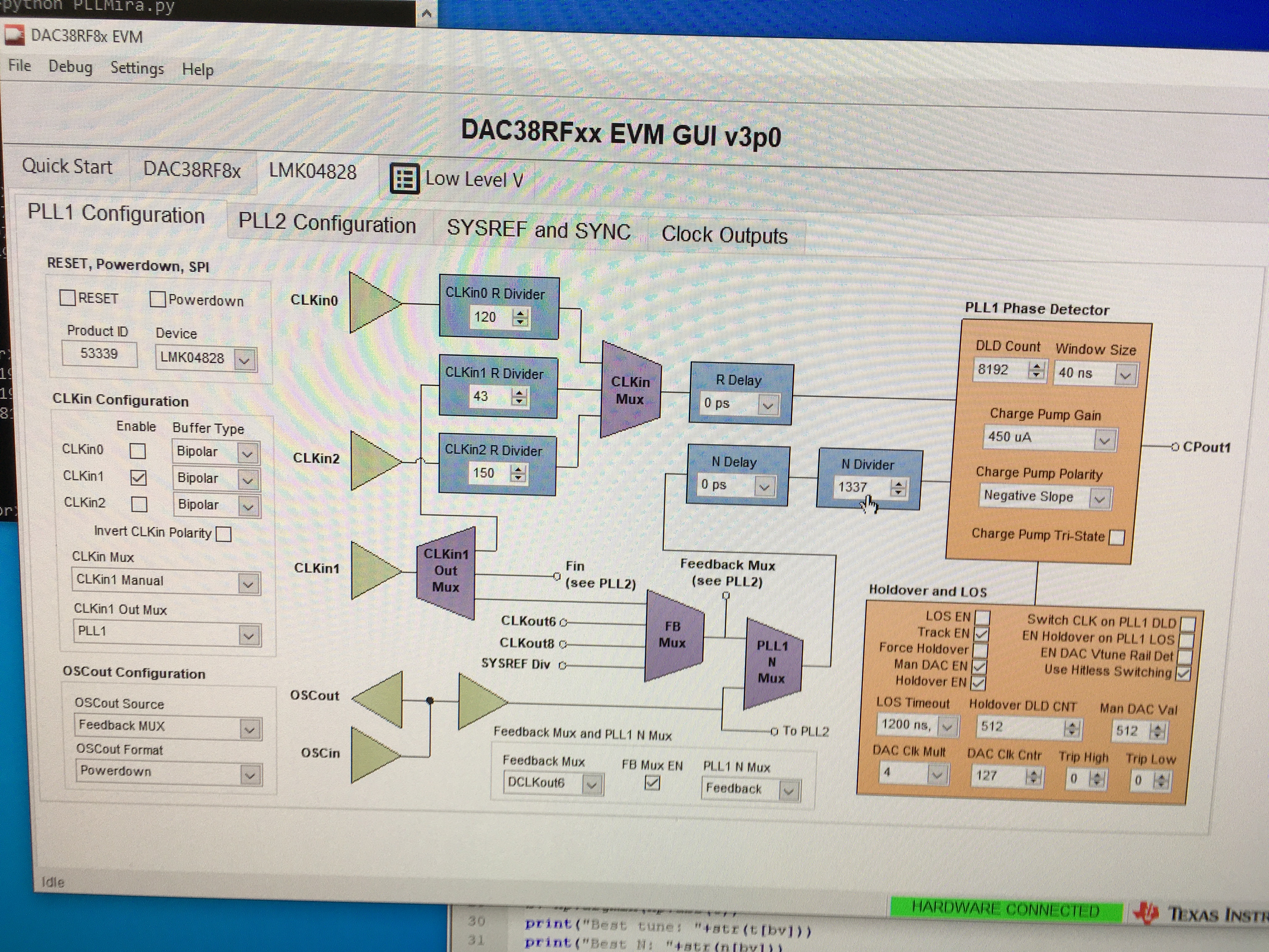
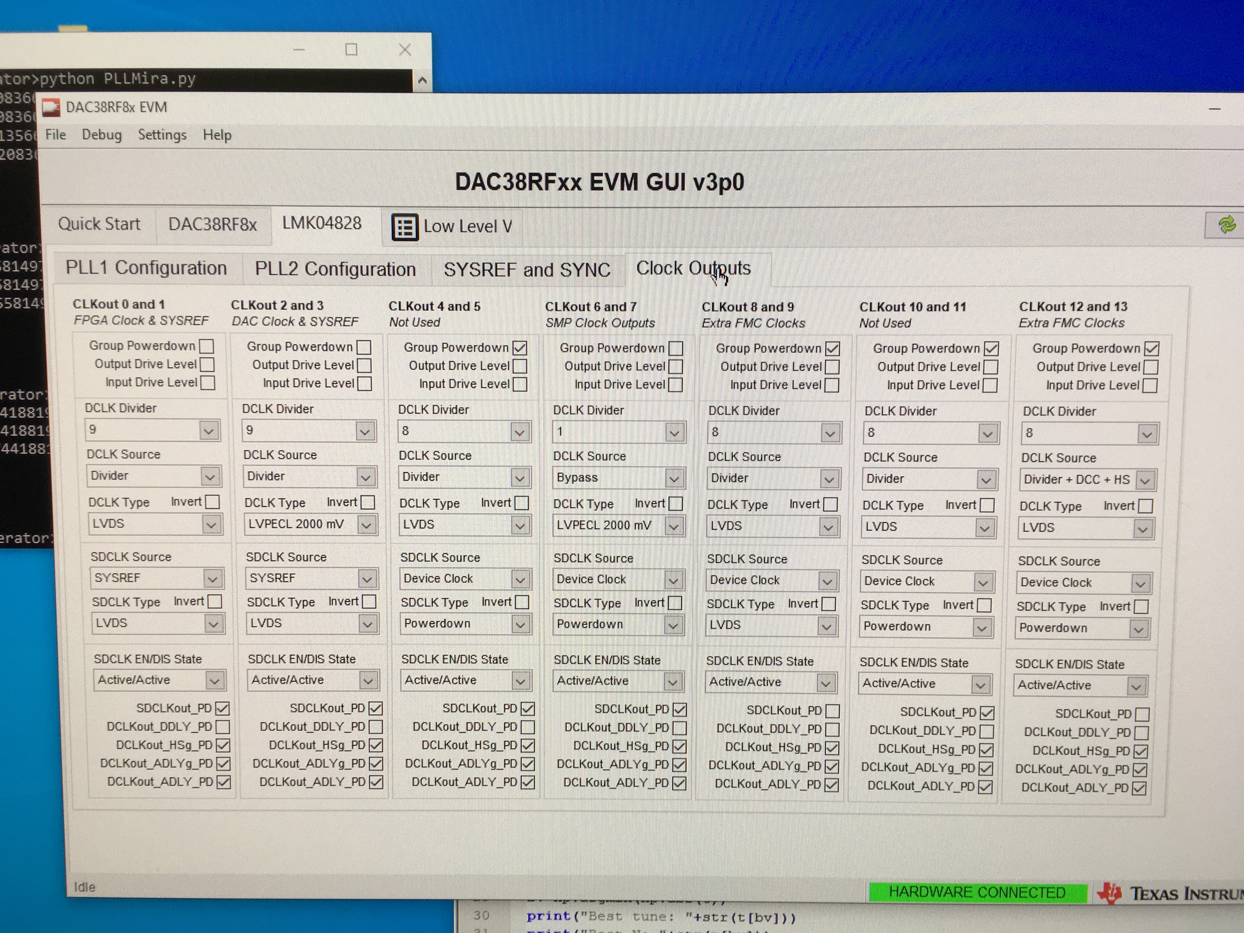
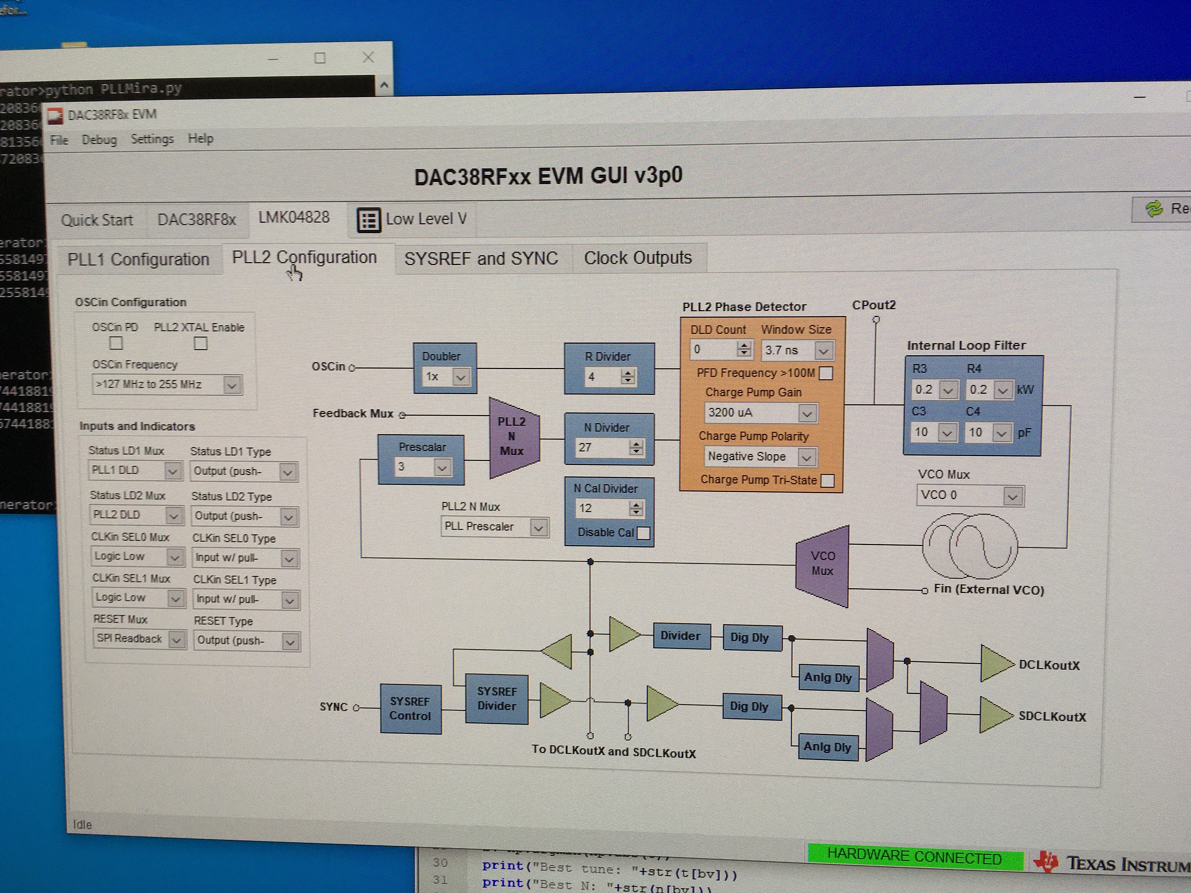
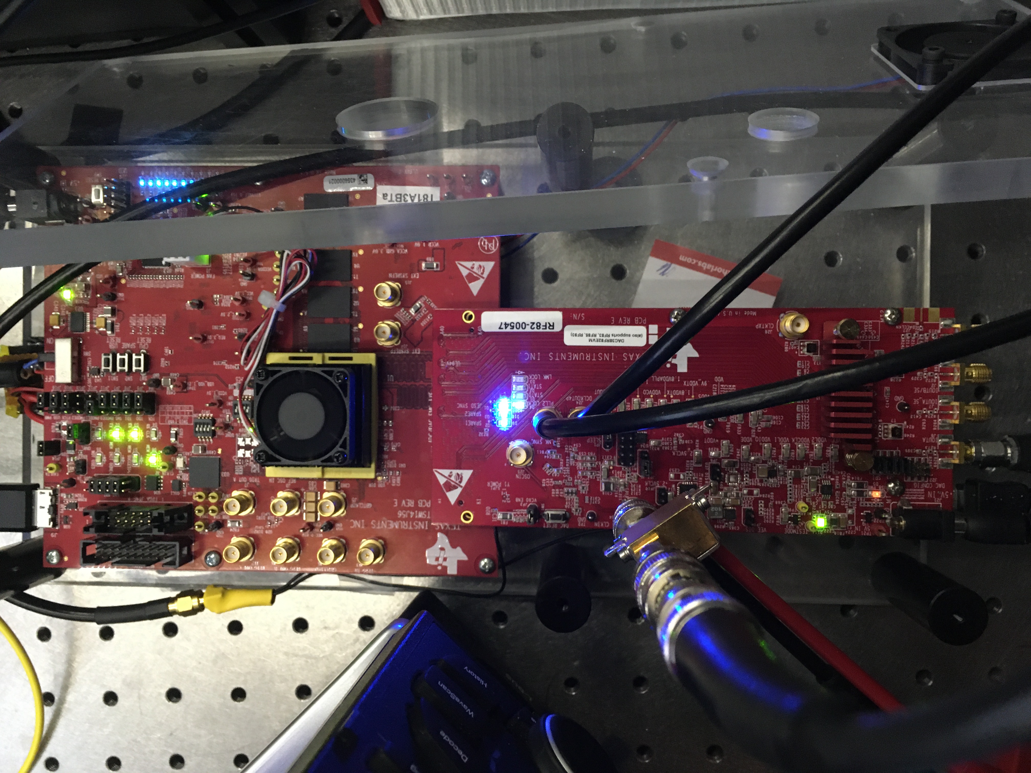
I am using a DAC38RF82EVM in combination with a TSW14J56EVM to run an optical experiment in which I want to synchronize the output data stream (8.84736Gsps) out of my dac (set according the configuration given below), to an external clock source given by the trigger of my pulsed laser which is running at 80.028MHz:

DAC38RF82_8847p36MSPS_PLL_8bitsmode_VCXO.cfg

My idea was to use a nested 0-delay dual loop to achieve fixed phase relationship between clkin1 (the 80.082 Mhz source of the pulsed laser) and the digital data at 8.84736Gsps converted by the dac.

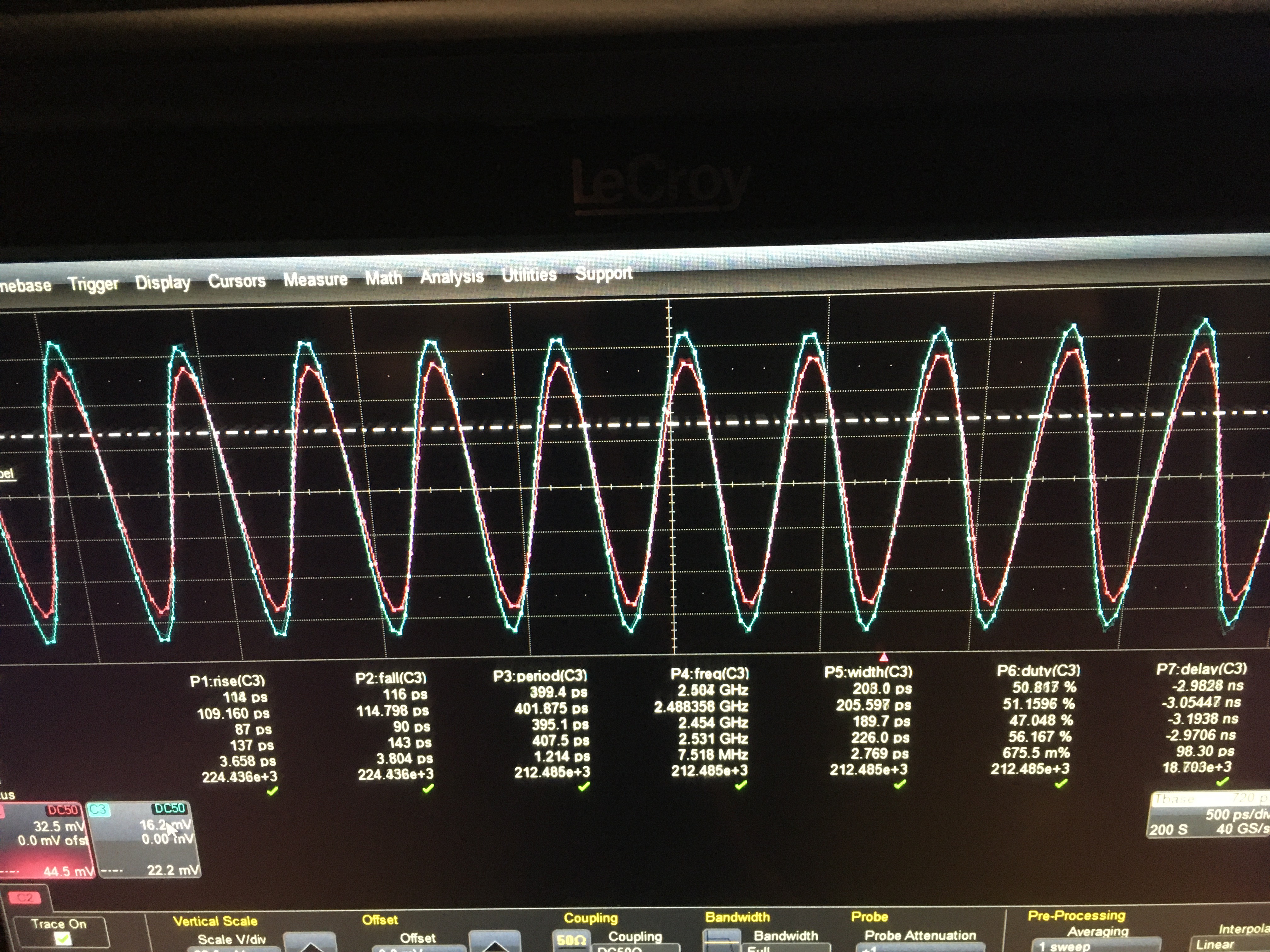
According to the parameters that i am setting  I get PLL1 LD and PLL2 LD turning green (the LD switches off when I unplug the laser clock off SMA J4). Therefore, I assume both PLL are locked and all clocks are in phase. Especially the dac sampling clock at 8.84736Gsps is in phase with my laser clock.

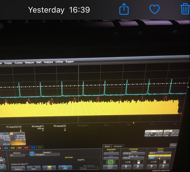
At this stage i generate a waveform which i send to a fast scope together with the laser clock. I would expect that, if locking is working correctly, the two pulses travel together but when i trigger on laser clock i see the generated waveform fluctuating back and forth. 

Can you help with this please? Can you suggest which settings I shall use in the GUI?

Thanks 

Antonio

  • Hello Antonio,

    Before we get into the configuration settings, I have several questions:

    1. Is the laser pulsed at 80.082 MHz or 80.028 MHz? I found both in the above. The 122.88 MHz VCXO cannot work with 80.082 MHz (N divider is too big), and I have seen some literature with 80.028 MHz lasers before, so I assume 80.028 MHz is correct.
    2. Am I understanding correctly that you are synthesizing a clock from the DAC at the same frequency as your pulsed laser, and so your theory is that the laser clock should have a constant phase difference with the same-frequency synthesized output of the DAC? Assuming your DAC pattern extends for (DAC samples/sec) / GCD(Laser Clock, DAC Data Clock) entries, I agree that the laser pulse would have constant phase offset to the DAC signal. 

    Additionally, in the configuration you sent, I observe the following:

    • FB_MUX is enabled and set to use DCLKout6, but DCLKout6 is not enabled (CLKout6_7_PD=1). The clock you are using for zero-delay must be enabled for zero delay to work. Therefore, the configuration is not locked to CLKin1. The only outputs I see active in this design are DCLKout0 and DCLKout2. (SDCLKout1_PD and SDCLKout3_PD are set, so no SYSREF is being sent on either. Also, SYSREF divide corresponds to 20/3 of data clock rate, does this value make sense for your application? Just double-checking.)
    • Additionally, for nested zero-delay, the output must be used as the feedback to PLL1. This requires PLL1_NCLK_MUX = 1, but in your configuration I see it is set to 0 (pulling feedback from the OSCin signal).
    • The CLKin1_OUT_MUX is not set to drive PLL1. It appears to be set to provide external VCO signals to the VCO_MUX.
    • Both PLL1_LD and PLL2_LD lights appear to be set to PLL2 LD. So it makes sense that both lights would turn green, even if PLL1 is not locked: if the VCXO frequency is active and close to correct, PLL2 should be able to lock to the VCXO output regardless of the settings for PLL1.

    I suggest the following modifications to the configuration file (assuming 80.028 MHz CLKin1 input):

    • 0x13F 0x09 (sets PLL1_NCLK_MUX to FB_MUX source, DCLKout6)
    • 0x147 0x1A (sets PLL1 input to CLKin1)
    • 0x155 0x00
    • 0x156 0xF7 (sets PLL1 CLKin1 R divider to 247)
    • 0x159 0x1E
    • 0x15A 0x00 (sets PLL1 N divider to 7680)
    • 0x11E 0xF1 (enable CLKout6_7, powerdown digital delay block (since it isn't needed), put OUT6 in bypass mode)
    • 0x11F 0x00 (set output buffer for DCLKout6 to powerdown, since 0-delay tap is before the buffer and buffered output format is not needed; see Figure 12 in LMK04828 datasheet)

    Regards,

  • Hi Derek,

    First of all, thanks a lot for helping. Coming to your questions:

    1) the laser is pulsed at 80.0823 MHz with standard deviation of 99.50 KHz (this is indeed what i feed to clkin1).

    2) That is exactly what i mean.

    The .cfg file in attachment was just to generate 8.84735Gsps signal out of the dac. The locking with the laser was not set in the .cfg because i did through the GUI. Sorry for that.

    Anyhow, i did cast all your parameters through the GUI

    • 0x13F 0x09 (sets PLL1_NCLK_MUX to FB_MUX source, DCLKout6)
    • 0x147 0x1A (sets PLL1 input to CLKin1)
    • 0x155 0x00
    • 0x156 0xF7 (sets PLL1 CLKin1 R divider to 247)
    • 0x159 0x1E
    • 0x15A 0x00 (sets PLL1 N divider to 7680)
    • 0x11E 0xF1 (enable CLKout6_7, powerdown digital delay block (since it isn't needed), put OUT6 in bypass mode)
    • 0x11F 0x00 (set output buffer for DCLKout6 to powerdown, since 0-delay tap is before the buffer and buffered output format is not needed; see Figure 12 in LMK04828 datasheet)

    Unfortunately, what i cannot do is to set PLL1 N-divider to 7680 (the max value allowed on the GUI is 4095). Is it a software problem or the N-divider can't be set so high for this product? for such  a reason i tried the numbers who closely match 2488.32 and 80.0823, namely N-divider = 1337 and R-divider = 43 even though 80.0283*1337/43 = 2488.32179302 which is not the exact value. You can check the pictures attached.

    What solution do you propose?

    thanks again

    Antonio

  • Hi Derek,

    i just made a new .cfg file e loaded it with the new settings. Now i can see the N-divider set to 7680. Nevertheless I cannot still see the pll1 green LED lighting up. I am wondering whether N-divider=7680 is actually set or the GUI just shows it. Can you please check if this .cfg is correct? lock9gsps.cfg

    Moreover i enabled clockout4(DCKL type = LVDS) with same settings as clockout6 and i see phase alignment between this and and LMK sync (namely, SMAj24 and SMAj8) which I expect to be correct.

    It seems just that the feedback clock at 2488.32Mhz can't lock to my laser clock source. Shall I play with the PLL1 Phase detector settings, R-delay or N-delay for phase adjustment?

    Thanks

    Antonio

  • Hi Derek,

    here is my last attempt of config file after playing with phase detector setting and holdover mode.

    locking_to_laser_attempt.cfg

    Unfortunately i do not see any improvements even though I still see the DAC Locked led on, the PLL1 and PLL2 LEDs turning on as well (but PLL1 led light is rather dim). For such a reason I have been playing with holdover settings since the LMK cannot find the locking conditions all the time. Anyhow, In order to check if locking was working at least partially, I generated one single pulse with the DAC to investigate the time histogram correlations between my laser clock to SMAj4 (pink trace) and the pulse generated with the DAC(blue trace) that you can see in the graph below.

    As you can see the histogram is completely flat meaning that the two traces are not correlated at all and one signal comes at random times compared to the other one.

    i wonder what is still wrong. May you please provide me with a good config file and give me an explanation for my mistakes?

    Best Regards

    Thanks in advance for your important reply

    Antonio

  • Hi Derek, can you please check my comments that I wrote below over the past  week? can you give me some more insight?

    Thanks

    Antonio

  • "... the PLL1 and PLL2 LEDs turning on as well (but PLL1 led light is rather dim)"

    It is possible that PLL1 can't lock well.

    "Unfortunately, what i cannot do is to set PLL1 N-divider to 7680 (the max value allowed on the GUI is 4095). Is it a software problem or the N-divider can't be set so high for this product? for such  a reason i tried the numbers who closely match 2488.32 and 80.0823, namely N-divider = 1337 and R-divider = 43 even though 80.0283*1337/43 = 2488.32179302 which is not the exact value"

    It is the reason. From reference, VCXO frequency, VCO frequency, we must match the exact frequency and integer divider. The EVM with 122.88 MHz is designed for wireless application. Maybe you can consider to change the VCXO for your application.