Other Parts Discussed in Thread: LMK04832, LMK04616, LMK00804BEVM, LMK1C1104, LMK00804B
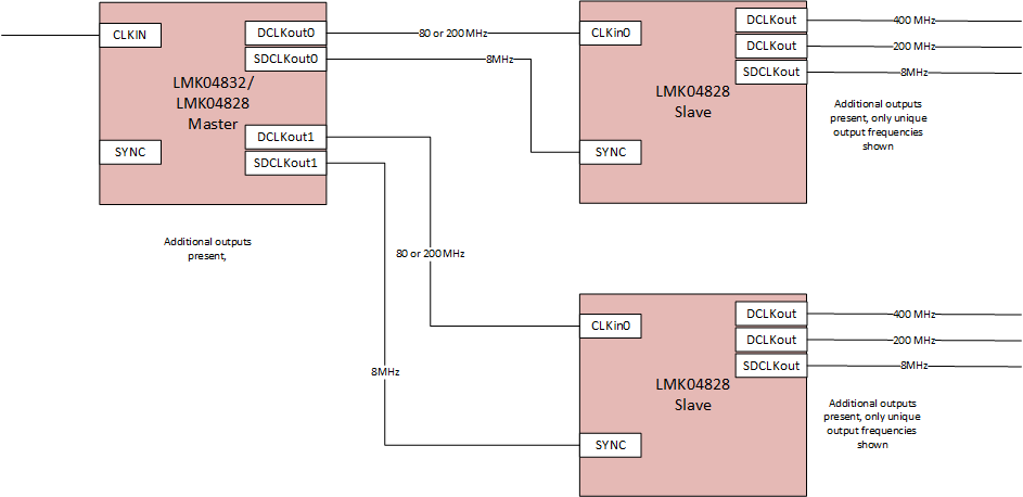
In a recent post, I was seeking assistance in deciding between a few different devices (LMK04832, LMK04828, and LMK04616) to serve as a master device driving two (eventually 4) slave LMK04828. Derek with TI did an excellent job conveying the characteristics of each. As that post was getting long, I wanted to create a separate post for discussing the output drive configuration of the master device. Simple block diagram below for context, followed by questions:
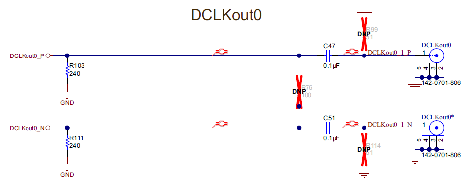
The master device, due to existing board constraints, must drive the slave devices through a single ended input to the slave board, AC coupled, that goes through 3dB attenuator before reaching the slave LMK04828 reference input. This means that any differential drive not involving additional circuits or balun would need to be terminated on the master board. The drive to the slave single ended input may be either 80MHz or 200MHz. Further, for our initial trials, the master board will be hosted on one of the existing TI dev boards. Please consider these points when answering my questions:
1. For the case of the LMK04832 as master, which is indeed what seems like the best fit, I am planning to use the LVCMOS output configuration to drive the slave LMK04828, this should require minimal change to the dev board output terminations. With the mentioned constraints, does this seem like the best choice?
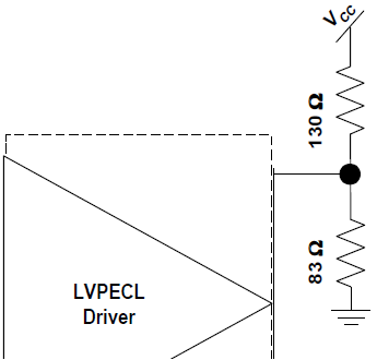
2. For the secondary case of using a 3rd LMK4828 as master, Derek reminded me that LVCMOS is only supported on OSCOUT. Derek mentioned using LVPECL (in context of another conversation) on LMK04828 to drive the AC coupled single ended reference input of the slave LMK04828s. I wanted to confirm with Derek or others if this would indeed be the optimal choice given the constraints we have as far as termination option.
Thanks