This thread has been locked.

If you have a related question, please click the "Ask a related question" button in the top right corner. The newly created question will be automatically linked to this question.

LMK04828: LMK04828 Multiple Device Sync Clock Tree

Part Number: LMK04828
Other Parts Discussed in Thread: LMK04821, LMK04832, LMK04616, LMK04610

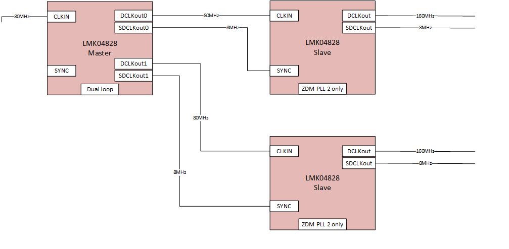
Consider the case where we wish to synchronize the outputs of two slave LMK04828 devices, both fed by an upstream master LMK04828

One LMK will act as master, and two will act as slaves.  We require matched deterministic phase through each of the paralleled slave LMK04828 devices.  The figure below hopefully provides clarification

Some questions

1. With the frequencies shown  in the diagram, and the two slave LMK04828s in ZDM PLL2 only config, will the phase through the two slave devices be matched and deterministic? 

2.  As the 80MHz clock into the slave devices is of course greater than the lowest output clock freq  (8MHz Sysref clock),   My thought is that I will need to use ZDM with re-clocked divider reset or SYSREF to obtain matched deterministic latency, across the two slave devices. is this correct?

3.  Would I be better of providing the slave devices with an 8MHz CLKIN and SYNC, and using the slave devices in Nested 0-delay Dual Loop mode?

Thanks!

  • Hello usethewrench,

    1. The phase between the two devices will be deterministic (in the sense that there are N possible phases between one slave device and the other, where N is the slave PLL2 phase detector frequency divided by 8 MHz), but whether the phase is consistent depends on the phase detector rate and the SYNC strategy. There are two ways to get consistent phase between the two devices:
      1. Set PLL2 phase detector to 8 MHz, guaranteeing all clocks align. Use SYSREF divider as ZDM feedback, forcing PLL2 phase detector rate to 8 MHz or lower.
      2. Use the SYNC to reset the slave devices, ensuring that the dividers all begin counting at the same time, and come up with a way to SYNC against a ~3GHz VCO.
    2. You can re-clock the SYNC signal to the SYSREF divider. However, unless you can meet ~300ps setup time on CLKin0 to re-clock the initial SYNC event against the slave device VCOs, you will still run into a problem ensuring that the SYSREF dividers are aligned to the same phase between slave devices - a "chicken and egg" problem. One way to solve this new problem is to set the internal SYSREF divider on the slave devices to 80 MHz and use it as ZDM feedback for PLL2. Then you can re-sync the device clocks against the internal SYSREF divider which is guaranteed to be aligned to the CLKin edge on each slave device, avoiding the chicken and egg problem and also permitting a higher phase detector rate on PLL2. To get the actual 8 MHz SYSREF, just reconfigure the slave SYSREF muxes to forward CLKin0 to SDCLKoutY, and connect the master SYSREF to the slave CLKin0. The master or the slave can be used to make any additional delay adjustments. To make things even easier, use CLKin0 as both the SYNC source and the SYSREF source, and use the master SYSREF pulser to generate a single SYNC event to all devices. No connection to SYNC pin is required.
    3. Nested ZDM could also work. There are three major differences between the above solution and a nested ZDM solution:
      1. Nested ZDM would "just work" without needing external divider SYNC, as you could arrange for only one phase to be possible between input and output. The PLL2-only solution requires a SYNC event, and arranging it is somewhat elaborate.
      2. Nested ZDM could avoid propagation delay differences in the CLKin0->SDCLKoutY path, which could move the SYSREF edge by a few tens (maybe low hundreds) of picoseconds across PVT. The PLL2-only solution might require some kind of compensation for SYSREF, if the edge timing is critical to within a few tens or hundreds of picoseconds.
      3. Nested ZDM costs an additional VCXO per slave device. The PLL2-only solution would be cheaper, lower power, and is probably sufficiently accurate for setting up a SYSREF for a 160 MHz clock even with some minor propagation delay differences in SYSREF timing.

    Regards,

  • Hello Derek,

    Thank you for your reply.

    Please consider my follow up questions (organized according to the question/response numbers we have used thus far), :

    NOTE: At least for the near term, for the 2 slave LMK04828 devices, the only PLL1 Reference Clock Input port available is CLKin0 ( CLKin1 and CLKin2, are not routed to external connectors).  This is what is driving me to use the SYNC input.

    1. (ZDM PLL2-only config, with SYNC input) - My apologies, my initial question #1 was meant to include that a SYNC signal, synchronous to the 80MHz CLKin, would be driven by the master to each of the slave devices.  Fortunately, your response spoke to such a case. 
      1. (I recognize you know this, and only included the option to help exhibit the point ) Using a PLL2 PFD frequency of 8MHz is not desirable
      2. In summary, to make the question #1 option work would require a SYNC to meet timing with the slave VCOs)

    2. I appreciate your suggestion of setting internal SYSREF divider on the slave devices to 80 MHz and use it as ZDM feedback for PLL2, and synching device clocks to SYSREF divider.  Do you see any problems with this approach given that the only  Reference Clock Input port available for the two slave devices is CLKin0, and that I would have to use the actual SYNC inputs on the slave devices?
    3. Nested ZDM sounds like it may be the best solution, putting power and cost aside, would you agree the nested ZDM would be the highest performing and simplest solution (given the device we are discussing and the board constraints I mentioned)?

    Two more quick follow on /related questions (number 5 is motivated by inability to adjust external loops filter components in near term for the slave devices)

    4.  If I wanted to apply the approach you suggested in  #2 topic (with the SYSREF muxes forwarding SYNC to SDCLKoutY) to a nested ZDM approach (but lets say with a 40MHz input for example)  My thought is yes, but just checking

    5. If I were to generate the 160MHz DCLK and 8MHz directly out of the Master in dual PLL mode, and distribute to the CLKin and SYNC inputs of the Slave devices that were configured in distribution mode , I would expect matched delay between the two slave devices, yes? I expect this would require some manual delay adjustments on the sysref paths, but those would be the same between the slave devices.

    Thanks

  • Hello usethewrench,

    Thanks for your patience, someone from the team or myself will get back to you on your questions.

    Thanks,

    Vibhu

  • I appreciate the heads up and am looking forward to it

  • Hi usethewrench,

    Apologies for the delay:

    1.  Yes, you would need to SYNC against the slave VCO timing.
    2. I don't see a problem with using the SYNC pin to assert the SYNC event, because the setup time for the SYNC pin is around 4ns, whereas you have 125ns window to target the SYNC event.
    3. I think that nested ZDM is the simplest solution with the setup you provided.

      If you did have a way to send the SYSREF signals from a slave device to the master, then in theory you might be able to set up the master for zero-delay mode with external feedback from a slave device on CLKin1 and a reference signal on CLKin0 or CLKin2 of the master. Then only the master would need the 8MHz phase detector, and any SYNC event that you issued to the slave devices should behave determistically on all the slave device dividers if the slave devices are in ZDM at 80MHz. However, I haven't confirmed this, and I don't know if resetting the slave device ZDM feedback dividers is precise enough through the SYNC pin to guarantee that all the SYSREFs will be at the same phase.
    4. Yes, I think it should still work. The advantage of #2 setup is that it allows the SYNC event to be timed against the input phase, regardless of how many PLLs come between the device input and output.
    5. Assuming the same temperature, voltage, and lot code, this would be true. However, differences in PVT between slave devices will cause differences in propagation delay. You could characterize each slave device for process, and track temperature on each slave device, but voltage variation is hard to account for. While our data suggests the Fin path delay variation across PVT in distribution mode is roughly comparable to the nested ZDM delay variation, we have no data on the CLKin0 to SDCLKoutY variation.

    Regards,

  • Thank you for getting back to me and for answering my follow up questions.  I have 1 left.

    For the architecture we have been discussing, the two slave devices are constrained to be LMK04828, but there is flexibility for the master to use an LMK04832, or perhaps an LMK04821.

    If I do use the Master's PLL2, I do not anticipate ever needing VCO greater than 2GHz, with all my foreseen output clocks being one of the following depending on the design(only one of these for a given design): 200MHz, 250MHz, 400MHz.

    For the master then, does the seemingly improved overall performance of LMK04832 become best choice, even though I would have to operate it with higher VCO of 3GHz and higher N2 value?  Or would I be better off  sticking with the LMK04828 or LMK04821 for the master to benefit from it having a nice VCO range around 2GHz?  I have also been looking at the LMK04616 to see how t fits into this mix.

    I am working through simulations between the LMK04828 and the LMK04832 for a few different approaches, but I cannot readily do so for the LMK04821 and LMK04616, and I need to purchase within a couple days.  With this in mind, If you can point out any discriminating factors, recommendations, or guidance for choosing a Master between the LMK04828 (or LMK04821), LMK04832, and LMK04616, I would be grateful.  (I also shouldn't have any more questions for a while =). 

    Thanks!

  • Hi usethewrench,

    1. Based on some PLLatinum Sim data, I expect around 85fs RMS 12k-20M @ 250MHz from LMK0482x, and around 60fs RMS 12k-20M @ 250MHz from LMK04832. I would not expect there to be much overall difference between LMK04821 and LMK04828, since you will likely be more limited by PLL noise than VCO noise.
    2. The LMK04610 is a smaller version of the LMK04616 that may better suit your needs. That said, the learning curve on these devices can be steep, especially for the supporting software. Judging by the datasheet plots at 245.76MHz, I think performance around 60fs should be achievable, which is comparable with LMK04832. However, it is worth pointing out that the LMK0461x achieves this in about half the total power consumption (by using 1.8V power supplies for the output supply pins). If you are short on time after purchase, or if adding an extra 1.8V supply to the system would complicate development, I do not recommend LMK0461x devices unless you believe the difference in power consumption could make it worthwhile. 

    If 25fs of performance improvement is not sufficiently compelling, there might be better volume pricing using 3x LMK04828 than 2x LMK04828 + 1x LMK04832. Likewise, 3x LMK04832 might be desirable. You stated that slave devices must be LMK04828, but just in case there is some undiscovered leeway, LMK04832 is p2p compatible with LMK04828 and should be able to generate the 160MHz output. The only potential wrinkle is that CLKin0 does not bypass reclocking by PLL2 VCO on LMK04832, which could introduce ~300ps uncertainty in the SYSREF timing. Food for thought, at least.

    If you do have more questions, I'll be happy to help.

    Regards,

  • Hello Derek,

    That was very helpful, thanks for the insight.

    When you said "the learning curve on these devices can be steep, especially for the supporting software," was that comment specific to the LMK04616 and LMK04610, meaning they are more of a handful than the LMK04828/LMK04832, or were you simply saying that using the LMK04616 would mean learning about an additional family of devices?

    I guess one more issue, unfortunately, for the hardware I have available in near term, the slave LMK04828 devices are setup to receive only single ended reference clocks.  It looks like the LMK04616 wouldn't be able to drive that as well as the LMk04832, speaking in terms of the max frequency it can drive single ended and the  span of the available input  voltage range it would use (speaking in terms of directly driving), which could be rephrased for this discussion as saying the LMK04616 slew rate would be lower, and thus the phase noise would be degraded. That sound right?

    Thanks

  • Hi usethewrench,

    The LMK0461x family uses a "semi-digital" PLL approach, which behaves somewhat differently than other PLLs, and as a consequence the diagnostic steps required when debugging issues diverge in occasionally surprising ways from typical analog PLLs. The support software includes a large number of settings for which there is little or no corresponding datasheet explanation. Once over the design and debugging hurdles, the LMK0461x perform admirably; but getting to this point is rarely as simple as putting frequencies in textboxes, loading the registers, and getting the desired results.

    Single-ended clocks are generally more susceptible to noise, whereas differential clocks have higher common-mode noise rejection. This shows up as close-in phase noise. But signal swing and slew rate are not necessarily linked. If signal swing is increased and rise/fall time is held constant, slew rate will improve. Likewise, if rise/fall time is reduced, and signal swing is held constant, slew rate will improve. As long as the clock driving the LMK04828 meets the minimum swing and slew rate requirements, there is no great advantage to increased amplitude (except potentially noise immunity, but if you have noise that exceeds the minimum amplitude requirements, you probably have bigger problems...).

    As for driving LMK04828 with single-ended LMK0461x output, it could be done by using the HCSL output format, terminating the unused leg of the differential pair at the IC, and AC-coupling the other leg to the LMK04828 OSCin. This is functionally not much different from using LVCMOS on LMK04832, or using LVPECL AC-coupled on LMK04828, as the driving source for the slave devices, and it satisfies the minimum single-ended swing and slew rate requirements.

    Regards,

  • Certainly I am with you as far as slew rate being a rate of change, but it didnt appear to me that the LMK04616 LVCMOS Tr and Tf were any shorter (for the same load, the 4616 datasheet load specifies less than half the capacitance  specified in the the LMK04832 datasheet) , with relatively similar or longer Tr and Tf assumed, it would seem that the lower swing would give lower slew. 

    You mentioned the idea of meeting the minimum slew rate, do we not expect performance to start to drop off with slew rate well before we reach the minimum?  Certainly you didnt say otherwise, but I imagined I should stay well above the lower limit.

    Thank you for your suggestion regarding the HCSL.  The situation is compounded by the slave boards have available for the near term, the reference clock provided to the slave boards is put through a 3dB attenuator.

    By "terminating the unused leg of the differential pair at the IC"  I would think you mean to do this near the LMK4828, correct?  Unfortunately that is not feasable because the slave board interconnect only accommodates a single ended input.

    To finish off, unless there are any surprises in your next response it seems like the LMK04832 is the best choice for us (please do let me know if you think otherwise from what we have talked about). 

    Thanks again

  • As far as I'm aware, LMK04832 does not have any rise/fall specs for LVCMOS in the datasheet. The closest I could find is LMK04828, specifying around 400ps typical into 50Ω 5pF, vs. 160ps/270ps rise/fall typical into 2pF (no resistance) for LMK04610. Approximating with I = C * dV/dt, I get 14mA from LMK04610 and 24mA from LMK04828, so while the LMK04828 value comes close to the expected peak current, the LMK04610 appears to be off by a factor of 2. So it's possible that the load capacitance of the LMK04610 could be incorrectly specified? At any rate, LVCMOS on LMK04828 and LMK0461x can only come from OSCout, so I'm not sure how relevant it is your use case.

    Yes, performance does degrade before slew rate reaches the minimum value. We even have a note in the datasheet, suggesting that while the minimum verified value is 0.1V/ns, the practical minimum should be considered 0.5V/ns or higher:

    Whether the output performance is degraded becomes a function of how much common-mode noise is present on the CLKin pins, and whether any degradation will be observable over the baseline reference input noise. If your reference is 3V/ns but the 10Hz offset comes in at -40dBc/Hz (to pick an arbitrary high value), the error introduced from reducing the slew rate will likely be much less than the inherent noise of the reference. If there's a summary guidance from this discussion, it should be: aim for the highest practical slew rate you can get.

    Ideally if you could terminate at the LMK04828 this would be most helpful, but practically if you only have one interconnect it must be done at the generating source. The HCSL trace would be run single-ended to the LMK04828. The other trace could be terminated near the LMK0461x. Running a differential trace part of the way and terminating far away from the device doesn't make much sense, since the impedance mismatch created by transitioning to single-ended at the interconnect between master/slave boards would likely be more disruptive than just running the trace single-ended and terminating the unused leg near the LMK04610. Again though, this may not be relevant if you're planning to move forward with LMK04832.

    It seems to me that the LMK04832 is the best choice.

    Regards,

  • Thanks for everything!