This thread has been locked.

If you have a related question, please click the "Ask a related question" button in the top right corner. The newly created question will be automatically linked to this question.

LMK04828: Multiple RFSoc Clock Tree Synchronization

Part Number: LMK04828
Other Parts Discussed in Thread: LMX2594, TIDA-01023, LMK04832

Hi All,

We're designing a system that will have 8 Xilinx RFSoc modules that will all need to be synchronized.  I've been told by Xilinx reps that the converter synchronization structure for the RFSoc behaves as a JESD204B converter does.  The 8 modules (each with an RFSoc) will be mounted on a single, central compute board that will be responsible for distributing common signals and clocks.  

The preliminary design needs to have clocks in the 156.25 MHz family and the module RF clock frequencies are:

  • ADC & DAC REF Clk = 312.5 MHz
  • PL REF Clk = 156.25 MHz
  • PL_SYSREF & RF_SYSREF = 9.765625 MHz  (this frequency must be < 10 MHz per Xilinx).

The requirement is to have all of these individual clocks synchronized and phase aligned not only in the module, but also across all modules.  The target is < 50 ps of jitter with the minimal amount of phase skew possible.  I've read multiple posts on this forum regarding the LMK04828 in zero-delay mode and I believe this is possibly the best solution, but I'm not sure if these frequencies are possible and what zero-delay mode would be best to use. I've been using the TICS pro software but it will not allow me to hit these frequencies and I'm not sure of the best VCXO frequency to use.  Any thoughts and values for these would be awesome.

Below is an overview diagram of the current thoughts:

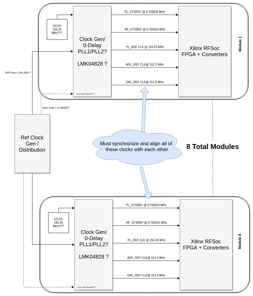
If all LMK04828 modules are in zero-delay mode and are being fed by the same reference clock, is it necessary to have an input sync signal?  

Thanks for the time in advance,

-Jim

  • Hi Jim,

    The LMK04828 TICS Pro logic is a bit squirrely. It helps to start from CLKinX and work forward through the signal path to set the desired frequencies. So for your example, I started with a reference frequency of 100 MHz, a VCXO frequency of 100 MHz, and a VCO frequency of 2500 MHz on VCO0. This makes a clock output of 312.5 MHz (divide by 8) and 156.25 MHz (divide by 16) on the DCLK outputs, and 9.765625 MHz (divide by 256) on the SYSREF outputs. Note that there is nothing special about 100 MHz, and you can use any reference frequency that generates an integer divide of 2500 MHz.

    One thing to consider: your jitter requirements are two orders of magnitude more relaxed than what the LMK04828 can usually achieve. You may not need to use PLL1 at all, since this is usually used as a low phase noise reference for PLL2. You could power down PLL1 and apply the reference directly to OSCin. Again, any reference frequency can be used, as long as it is an integer divide of 2500 MHz. That being said, some choices are better than others; I elaborate on this below.

    Regarding "Is it necessary to have an input sync signal?": There are three good reasons to use an input SYNC signal:

    1. When PLL_N / PLL_R is not an integer value. In this case 0-delay cannot be used without a divider reset, which is delivered on the SYNC/SYSREF path.
    2. When configuring digital delays to align the SYSREF and clock outputs. Useful for trimming out routing delays or aligning the SYSREF output to the center of a valid window on the data clock.
    3. When using the SYNC input as a SYSREF request, or a trigger to the SYSREF pulser. In this case, the input SYNC signal is not used to trigger a divider reset, but it can trigger the pulser circuit or it can be reclocked to the downstream SYSREF clock.

    In your case, you could set the phase detector frequency to the SYSREF frequency, and use the SYSREF divider as the PLL2 feedback frequency. Then set the reference equal to the SYSREF frequency. In this configuration, there is only one valid phase, so a divider reset is not required to guarantee phase determinism. However, the phase detector frequency is less than 10 MHz, which can impact the phase noise. If your jitter requirement is really only < 50ps, reduced phase detector frequency probably doesn't matter in your application. There are still the two other reasons why it might be a good idea to use an input SYNC signal, but you should have enough information now to decide whether those reasons are compelling.

    Regards,

  • Hi Derek,

    Thank you for the response and the great information.  

    The design has changed a little and now we will have (3) LMX2594's between the slave LMK04828 and the RFSoc.  These will now be responsible for supplying the sampling clocks directly to the RFSoc and therefore will also have to all be aligned. 

    1. I've read TIDA-01023 and it seems very similar to what we're going after, but the slave LMK04828 is being used in distribution mode instead of 0-delay mode, do you see a major issue with this and synchronization between slave LMK04828's?  Is distribution mode preferred over 0-delay mode for this application when the clocks are all sub-multiples of each other?

    2. In the diagram below from TIDA-01023, the CLKin0 of the slave LMK04828's is being used to synchronize the outputs, but is this a continuous free running clock running at a sub-multiple of the input reference clock (CLKIn1)? Or is this a single pulse from the master that is asserted upon initialization from the SYNC pin (or register) on the master? 

    3. Also from TIDA-01023, in the diagram below the slave LMK04828 is being used to synchronize all of the LMX2594's via the SYNC pin.  Is this signal a continuous free running clock at a sub-multiple of the reference frequency to the LMX2594?  Or is this a single pulse that is applied when the SYNC pin for the slave LMK04828 is asserted?  

    4. Are the .tcs files for the clocks from TIDA-1023 available somewhere?  It would be very helpful to go through and see exactly how things are setup in the GUI.

    Thanks again for your help through this learning experience.

    -Jim

  • Hello Jim,

    Sorry for the delay in getting to your post.

    I did want to make a comment on SYNC.  When it comes to high performance synchronization, I always consider it best to use CLKin0 for driving SYNC to the internal dividers or down stream.  It is possible to use the SYNC pin, but it is a CMOS pin and subject to more skew.  Note that TIDA-01023 uses SYNC for the 'top level' SYNC request, but then downstream LMK devices receive the SYNC/SYSREF on CLKin0.

    James Tasker said:
    1. I've read TIDA-01023 and it seems very similar to what we're going after, but the slave LMK04828 is being used in distribution mode instead of 0-delay mode, do you see a major issue with this and synchronization between slave LMK04828's?  Is distribution mode preferred over 0-delay mode for this application when the clocks are all sub-multiples of each other?

    I don't see a major issue.  Using the device in distribution has less propagation delay variation over temperature, 140 ps in distribution mode vs. 170 ps over temp for PLL2 only 0-delay mode.

    As you point out, since all your clocks are low frequency and sub-multiples, I expect the absolute best performance could be achieved with a single 312.5 MHz VCXO (or just XO) in a master clock distribution (which could be an LMK04828), then allowing the downstream LMK04828 to re-clock the input SYNC/SYSREF.  Again if you use an LMK04828 for the master clock distribution, it could generate the SYSREF and distribute it to the downstream LMK04828 which could then re-clock this SYSREF.
      * Using this approach (without PLL2), you lose the ability to adjust digital delay in half high frequency VCO cycle steps, instead digital delay will be in half cycles of the low input frequency of 312.5 MHz.  But that's ok because you can use analog delay to position the SYSREF into the 312.5 MHz clock which has a relatively large period.
      * One disadvantage of this approach is that your noise floor wouldn't be as good as if you used PLL2, but the close in noise would be much better because you're not adding PLL2 noise to do frequency multiplication.

    James Tasker said:
    2. In the diagram below from TIDA-01023, the CLKin0 of the slave LMK04828's is being used to synchronize the outputs, but is this a continuous free running clock running at a sub-multiple of the input reference clock (CLKIn1)? Or is this a single pulse from the master that is asserted upon initialization from the SYNC pin (or register) on the master? 

    It should just be a single pulse.  There is some pipe-lining so if you kept resetting the output clocks, you wouldn't have a good output waveform.

    James Tasker said:
    3. Also from TIDA-01023, in the diagram below the slave LMK04828 is being used to synchronize all of the LMX2594's via the SYNC pin.  Is this signal a continuous free running clock at a sub-multiple of the reference frequency to the LMX2594?  Or is this a single pulse that is applied when the SYNC pin for the slave LMK04828 is asserted?  

    I expect the SYNC pin is just requesting the SYSREF pulser to send out a SYSREF/SYNC pulse.

    James Tasker said:
    4. Are the .tcs files for the clocks from TIDA-1023 available somewhere?  It would be very helpful to go through and see exactly how things are setup in the GUI.


    I'll see if I can track them down.

    --

    Note one concept used for multi-sync of LMK04828 is to use ZDM with the SYSREF divider.  Then you program the SYSREF_MUX for re-clocked mode.  What this allows is a deterministic phase from the re-clocking clock at the SYSREF D flip flop to the reference.  So if you send the CLKin0 (or SYNC) signal on the falling edge of the reference, it will be re-clocked onto the 'vco domain' and will then be sent out the SYSREF clocks.

    * Please be aware of the LMK04832, a pin compatible clocking device.

    73,
    Timothy