This thread has been locked.

If you have a related question, please click the "Ask a related question" button in the top right corner. The newly created question will be automatically linked to this question.

SYNC pulse in Pulse Sync Mode - RDATAC

Part Number: ADS1282-SP

Hi all,

I'm using ADS1282-SP for the first time and I have to design the FPGA which controls it. Being the latter an OTP device I have no room for errors.

My intention is to use the ADS1282-SP ADC in Read Data Continuous (RDATAC) mode and in pulse-sync mode.

The datasheet reports two figures to compare pulse-sync with continuous-sync reading modes.

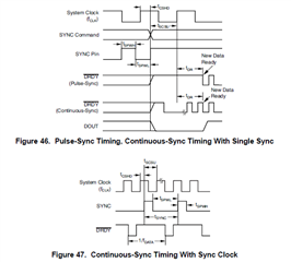
In continuous-syncmode is possible to use a clock-like pulse signal respecting all the constraints w.r.t. the ADC Clock. and it's very clear.

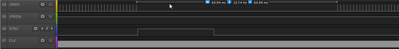
What I need to understand clearly is the form the SYNC pulse shall have when working in Pulse-Sync mode.

Shall ADC's SYNC input be driven high then low and then high again (w.r.t. timing constrains) or shall it be driven low-to-high only once to trigger a new conversion?

Shall SYNC pin stay high for all the time I am reading data and be driven low only when I don't need to read converted data output by the ADC? in other words, does SYNC pin have effect on enabling/disabling /DRDY output?

Waiting for your kind reply.

Best regards,

Daniele Lippi

  • Hi Daniele,

    Figure 46 shows SYNC going high-low-high primarily to include the timing information about the minimum SYNC pulse width (tSPWH and tSPWL). However, during normal use the SYNC signal is taken high to synchronize the ADC. SYNC is returned low sometime later (either soon after performing synchronization or prior to the next synchronization - the falling edge of SYNC doesn't perform any action so the timing of this edge is not critical so long as the the minimum SYNC pulse width timing specification is met).

    Here is an example waveform (though the pulse width here is much wider than it needs to be):

    Please note that the timing of the SYNC rising edge is important. The datasheet recommends at least a 10 ns setup time between the SYNC rising edge and the CLK rising edge. If this setup time in not met then the device may ignore the SYNC pulse and continue on-going conversions.

    • To avoid this issue, it is best to align the SYNC rising edge with the CLK falling edge. This can done using a flip-flop to re-clock the SYNC signal (a discrete solution could use something like the SN74HCS72, D-type negative-edge-triggered flip-flop).
       
    • Alternatively, if the SYNC and CLK signals are asynchronous, then I would suggest toggling the SYNC signal multiple times (similar to what is shown in Figure 46). It is generally a low probability for the SYNC and CLK signals to align when running asynchronously, and the probably of this happening two times consecutively is significantly lower, so toggling the SYNC pin twice is usually sufficient to ensure that synchronization occurs.

    Best regards,
    Chris

  • Christopher,

    in the meanwhile I had found the same information in the following discussion held in this forum some years ago: ads1282-ads1283-sync-issue

    Using an FPGA, I can obtain fine timing, so I'll opt for syncronizing SYNC commutation on either ADC_CLK's edge. ADC_CLK is not my system clock. I'll detect ADC_CLK's edge through an edge detector with a resulting setup time of 83.34ns and a hold time of 208.33ns in case of synchronization to falling edge, or vice versa in case of synchronization to rising edge.

    Thank you very much.

    Best regards,

    Daniele