This thread has been locked.

If you have a related question, please click the "Ask a related question" button in the top right corner. The newly created question will be automatically linked to this question.

ADS1018-Q1: ads1018-q1

Part Number: ADS1018-Q1
Other Parts Discussed in Thread: ADS1018, , ADS1118

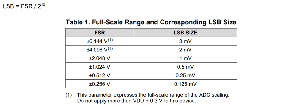
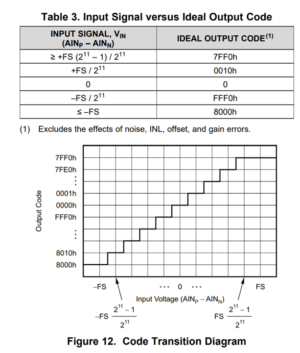
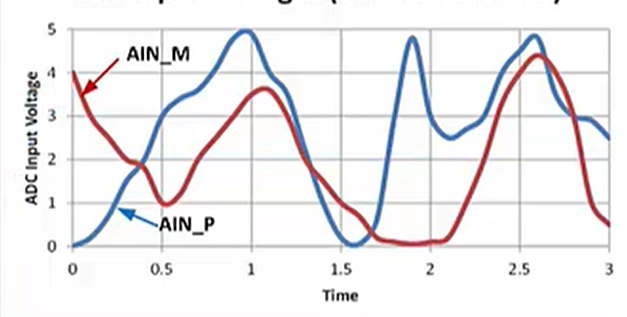
I wanted to understand how to calculate temperature from ADC counts , when we are configuring ADS1018 in ADC mode.

also I wanted to understand how ADC counts are co-related to ADC counts.

  • Hello TI, on forums not seeing any reply for my thread. request you to give me inputs so I can proceed. this is one of the priority . it will be real helpful if I get some directions

  • Hello Varsha,

    Thanks for posting on data converter forums! 

    Unfortunately, this question is a little vague so I'm going to make some assumptions in order to answer your question thoroughly.

    The assumptions are:

    • You have a sensor that measures temperature connected to the inputs of the device
      • I only mention this because the ADS1018 does have an internal temperature sensor. As a reminder, it is impossible to use the internal temperature sensor when TS_MODE = 0b (ADC mode). The internal temperature sensor can be accessed when TS_MODE = 1b
      • If you do have questions about the internal temp sensor, the "Converting from Digital Codes to Temperature" section which goes over its own equations as it does not depend on the PGA[2:0] setting
    • When you say "understand how ADC counts are co-related to ADC counts" I assume you want more information how the output ADC count is determined

    I'd say understanding the whole conversion chain from temperature to code needs two parts: the temperature to voltage equation from the sensor, and the voltage to code conversion.

    Temperature to voltage:

    The temperature to sensor voltage doesn't depend on the device, so you'll need this info from the sensor datasheet. As such, you might find an equation or a table in the sensor datasheet that shows the minimum differential and common mode voltage for the sensor outputs. 

    Using this info, we can refer to table 1 in the datasheet and pick a PGA setting:

    Typically, the full scale range (FSR) is determined by an equation that includes the PGA gain and the reference voltage, but the datasheet tries to make it easier for the user since the reference is fixed and PGA is internal. More info on that can be found in this post if you're interested: https://e2e.ti.com/support/data-converters-group/data-converters/f/data-converters-forum/907372/ads1018-q1-ads1018-q1 As a result, the user just needs to use the smallest FSR value that encompasses the voltage range (and therefore temperature range) that needs to be sensed. 

    The one thing I need to stress is that if the higher FSR values are picked, then the VDD and absolute maximum specs need to still be observed. Just because the table says 6.144V, doesn't mean that 6.144V can be applied to the inputs as VDD can't go to 6.144V. Its for scenarios where, for example, the sensor can go to 5V where the 6.144V can never be achieved, but 5V would never be sensed using the 4.096V FSR setting.

    I'll also note that using LSB = FSR / 2^12 to derive the LSB size column could result in some confusion. If you have never worked with negative numbers in context of ADC codes, I would recommend to keep reading as it'll be explained later.

    Voltage to code:

    Table 3 in the datasheet gives us an equation to go from voltage to codes but there are two key ideas to understand beforehand.

    The first is that codes can only be pulled from the device at 2 or 4 bytes (8 or 16 bits) at a time. This means the final code will have 16 bits or 8+8bits. Note, this is a 12 bit ADC which means the last 4 bits (or last byte) is worthless, always 0b, and does not convey real data. In other words, 0x7FF may be the equivalent largest positive code that utilizes all 12 bits, but a controller will have to receive 0x7FF0 because the packet has to be 16 bits long.

    The second idea is that the codes are in twos complement, left justified format. This means, AIN_P - AIN_N can result in a negative number and to represent that negative number, we designate the MSB to be the sign where 0b = positive number and 1b means a negative number. So using 2's complement conversion, you can understand the true value and add the sign after. These are reasons why we use 2^11 in the equation below and why the LSB calculation is twice the expected amount in table 1.

    .

    What the table and figure is trying to say is that the sequence from voltage to code is V_input = n_code*(FSR/2^11) -> 2's complement if negative -> add 0x0 to end -> get final code to be sent to controller.

    Going through an example, let's use FSR = +/-1.024 where the LSB is 0.5mV, and the input or AINP - AINN will be -0.5mV.

    n_code = (-0.5mV)*(2^11/(-1.024))

    • Note, I moved around the equation and used the negative full scale value because the input is negative

    n_code = 1 = 0b0000 0000 0001

    • Now need to do 2s complement because it was negative. Or flip bits then add 1

    n_code_2s = 0b1111 1111 1111 = 0xFFF

    • Add 0x0 on the end

    n_code_final = 0xFFF0

    Which equals the value in the table.

    Final note about errors and things

    The table doesn't account for errors, as determined by the footnote. If you need to review how errors get added into the final result, then please review the TIPL ADC series on errors and noise and check out the design section of the TI reference design Precision Thermocouple Measurement with the ADS1118 (which similar to the ADS1018-Q1 but 16 bits and with lower temp range) https://www.ti.com/lit/ug/slau509/slau509.pdf 

    Best,

    -Cole

  • Hello Cole

    thanks for the reply.

    Please do consider below points

    1. I have configured ADS1018 in ADC mode.

    2. below configurations I have done

    Mode = ADC

    010 = FSR is ±2.048 V (default)

    Pull Up enable

    Data rate = 2400

    supply voltage for ADS1018 is 5V

    I am performing 32 bit SPI communication and getting below response for config write 0x44AB 44AB

    0x64E0 44AA

    MSB is 0x64E0 (16 bit ADC counts ) LSB 44AA which config register read back.

    my question is how to convert ADC counts 0x64E0 to temperature value.

    I understand its 16 bit result buffer and 12bit will be result only so actual 12 bit result is 0x64E

    if I convert this to decimal it will be 1614

    0.125* 1614 = 210.75 deg  (which is invalid)

    please guide me how ADC counts 0x64E0 will be calculated to temperature value.

  • Hello Varsha,

    Here's my math:

    0x64e0

    • Chop off last 0

    0x64e

    • To binary

    0110 0100 1110b

    • Positive number, so no two’s complement. Now convert to decimal

    1614

    • Looks like you're here, time for equation

    V_input = n_code*(FSR/2^11)

    V_input = (1614)*(2.048/2^11)

    V_input = 1.614V

    You haven't given me an equation for the temperature equation (you also didn't specify which kind of degrees, though C is the industry standard). 

    I think we throw out the degrees to voltage conversion for now. Can you probe the appropriate input pins and see if you approximately have 1.614V for AINP - AINN? I just want to make sure our equation is right.

    Best,

    -Cole

  • Thanks Cole

    This will help. again one more question.

    I am giving 5V supply to ADS1018 , and default ±2.048 V. This is ok right?

    also as below above formula if I give 5V voltage then I am getting 0x7FF0

    if I go reverse with above formula

    then

    I will result into

    0x7FF = 2047 (decimal)

    V_input = 2047 * (2.048 / 2048) = 2.047V

    is it due to FSR range?

    what FSR is suggested for 5V input supply?

  • what I mean to say is if I am giving 5V as input voltage to ADs1018 then I am getting 0x7FF0 as counts is it valid? with above formula it will be 2.047V.

    so is that means I am selecting incorrect FSR? as I am giving 5V input supply to ADS1018

  • Hey Varsha,

    There's two bits here. The first is that the ADS1018-Q1 has a true differential input and the V_input is calculated as AINP - AINN. So, to be extra clear, when you're applying 5V, I assume you're saying that AINP = 5V and AINN = 0V or GND. 

    The second, is that this input exceeds the positive FSR. If we go look at table 3 again. When V_input > +FS(2^11-1)/2^11, or we're exceeding the positive FSR (which is V_input > 2.048V) we expect the code 0x7FF0. That's exactly what we're seeing because 5V > 2.048V. 

    Is there anything wrong with this? From a device damage perspective, no. Your VDD is 5V, and applying 5V to AINP will not cause any device damage. But its clear the device can't measure 5V in this configuration because you need a positive FSR > 5V to measure AINP = 5V and AINN = 0V. 

    As a result, if you would like to measure the AINP = 5V and AINN = 0V case, you'll need to change the FSR range to +/-6.144V. Something like this:

    Alternatively, if you're confident that AINP only changes from 0V to 5V and AINN can stay constant, then you can set AINN = 2.5V and use the +/-4.096 FSR and work out the math when AINN = 2.5V and AINP = 0V (or V_input = -2.5V) on the controller side. Something like this:

    However, this is not how most real temperature sensors work. Most temperature sensors a differential so AINN cannot be held constant. Something like this:


    So, take into account what your temperature sensor actually needs.

    By the way, these pictures are directly lifted from the ADC TI Precision labs series. It seems like you might benefit from watching these videos so I'll throw a link for you to explore:

    https://training.ti.com/ti-precision-labs-adcs-sar-adc-input-types?context=1139747-1140267-1128375-1139103-1128659 

    Best,

    -Cole

  • Thanks for all the detailed explanation Cole. This really helped . Thanks !