This thread has been locked.

If you have a related question, please click the "Ask a related question" button in the top right corner. The newly created question will be automatically linked to this question.

DAC39J82: Details on measurement setup for NSD & issues with Spurious

Part Number: DAC39J82
Other Parts Discussed in Thread: LMK04828

Hi,

We have ordered the Eval board DAC39J82EVM and have started the characterization.

We are trying to measure NSD in our LAB, but we are unable to meet the numbers due to equipment limitations.

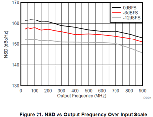
Since this is an important parameter in our design, we would like to know the measurement setup used for validating the NSD numbers mentioned in the DAC datasheet (Figure 21, Page no 21). Could you please provide the measurement setup and parameters used? NSD figure from Datasheet is attached below for reference

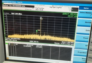
Another observation with DAC39J82EVM is while generating any output from the DAC, Spurious components are observed on both sides of Generated output at around 58-60 KHz offset frequency. These Spurious components are seen even when DAC is configured to generate LO output only (FPGA board is powered off and DAC generates LO @ 100 MHz). Are you aware of these spurious components and how to get rid of them? A Reference Snapshot is attached below.

Thanks,

Kiran

  • Hi Kiran,

    Please see attachment for NSD measurement. 
    NSD_Measurement.pptx

    I tried several frequencies and did not see a spur around the fundamental. From the FFT plot, clock source may not be as good since the noise floor moves up and down. what are you using for your clock? You need a clean signal generator to get the best results.

  • Hi Miguel Lomeli,

    Thanks for the response.

    Regarding Clock settings in the attached PPT document :

    • Please note that we are not using HSDC pro as we don't have/use the intermediate board (TSW14J10EVM)
    • What shall be the frequency and the power level of the External clock, will this clock be fed through J17? FYI, we are using DAC3XJ8X GUI for configuring LMK and DAC chips.
    • What are the additional Board settings like Jumper (JP2) to be made? do we need to mount/unmount any discrete components like Resistors/Capacitors in order to use external clock?

    Regarding "what are you using for your clock?", till now we are using the LMK04828 and the onboard 122.88MHz VCXO/crystal available on DAC39J82EVM for generating all the clocks. Do these spurs expected with this setup? Spurious components are seen even when DAC is made to generate LO output only (FPGA board connected over FMC is powered off) and these components are also observed on Clock output test points (Spurs @64 dBC). Could it be due to the regulators used for Supply(We are using default adaptor)?

    Thanks,
    Kiran

  • Can you send me screenshots of the Quick start, Clocking & Dig block tab. This will help me to understand your setup.

    When i tried the NCO, I couldn't reproduce the spurs. I also thought that you could possibly be using the PLL which then i tried that too with the NCO but didn't see any spurs, I'd recommend staying in bypass mode for the clock.

  • Hi Miguel Lomeli,

    Can you please check the Signal Analyzer settings, please note the settings that we have used in the spectrum screenshot sent earlier (RBW = 300 Hz, Video BW = 300 Hz, Span = 100 MHz with the Generated output as center frequency (Example 100 MHz) and please let us know on the captured spectrum.

    Also please note that our final application will not use NCO, but in order to study this Spur clearly, we have checked the following three outputs

    • DAC generating output based on data from the Baseband processor FPGA (say 100 MHz single tone), here 58 kHz-60 kHz Spurs are observed
    • Data from the Baseband processor is absent (its powered off), DAC generating output using NCO, here also the Spurs are present
    • Probed sampling Clock output of LMK04828, here also Spurs are present

    So by the looks of it, we feel this Spur should be either from the Supply Adaptor/regulators or from the LMK04828, do you have any reference plots of the EVM monitoring DAC/LMK outputs?

    In the previous response, you had mentioned "recommend staying in bypass mode for the clock", can you please elaborate more on which module and what settings must be kept in Bypass mode

    We will upload the Screenshots of the Quickstart window, LMK and DIG block settings shortly.

    Thanks,
    Kiran

  • Hi Miguel Lomeli,

    PFA Word and PDF documents having screenshots of the GUI for your reference. PDF format of the file was also attached just in case if you face any Formatting issues with the Word document.  

    Please let us know your feedback.

    Thanks,

    Kiran

    dac39j82evm_config_snap.docxdac39j82evm_config_snap.pdf

  • Hi Miguel Lomeli,

    One more doubt, on the final page of NSD_Measurement.pptx, one variable named Fund is used in the NSD equation, could you please provide more details on this in order to understand it better.

    Thanks,
    Kiran

  • Hi Kiran,

    Thank you for sending the pdf. It helped me to better understand your setup.

    If you wanted to use an external clock from the quick start tab in the choose clock mode click on the drop down and select external clock. Make sure that JP2 is disconnected as this jumper powers the onboard OSC.  Now you are ready to apply an external clock.

    The default for the DACCLK is bypass mode which you have select and I've added a slide to give you a visual.

    On the NSD_Measurement.pptx Fund is the fundamental frequency power in dbm.

    The picture that you have provided, is it with the NCO enabled or is it a modulated signal? I'm trying to understand why your noise floor is up and down. 

    Can you take your rf probe and probe the test points where the device supply test-points are? Usually spurs this low are due to regulators. This will tell us where your spurs are coming from.

    attachment pptx has FFT plots showing no spurs within 1MHz range of fundamental.  I've attached the schematic for the evm. as well 

    AC_Spur_Near_Fundamental.pptx7288.DAC3XJ8XEVM-SCH_D.pdf

  • Hi Miguel Lomeli,

    Thank you for providing your feedback, please find  the response inline

    If you wanted to use an external clock from the quick start tab in the choose clock mode click on the drop down and select external clock. Make sure that JP2 is disconnected as this jumper powers the onboard OSC.  Now you are ready to apply an external clock. : How to configure the Clock GUI with arbitrary input clock frequencies? or In external mode are we suppose to provide the DAC Sampling clock directly (if DAC sampling is 1.2 GSPS, provide 1.2 GHz clock @ LMK input), LMK used for distributing the clock?

    The default for the DACCLK is bypass mode which you have select and I've added a slide to give you a visual. : While using Onboard clock (and LMK deriving the required sampling clock) we have kept DAC PLL in sleep mode, and our configuration matches the "Check if bypassing PLL or using External Clock" slide of the PPT

    On the NSD_Measurement.pptx Fund is the fundamental frequency power in dbm. : will come back on this point

    The picture that you have provided, is it with the NCO enabled or is it a modulated signal? I'm trying to understand why your noise floor is up and down.  : This is with DAC's NCO enabled, here modulated data is absent and FPGA Board is powered off

    Can you take your rf probe and probe the test points where the device supply test-points are? Usually spurs this low are due to regulators. This will tell us where your spurs are coming from. : We will check across TP29-TP27 & TP19-TP9 and come back on this point

    attachment pptx has FFT plots showing no spurs within 1MHz range of fundamental.  I've attached the schematic for the evm. as well  : What is the supply source in this setup? Are you using the Adaptor which comes with the DAC EVM? We tested with the const input box Checked without any improvements, Spurs are observed here as well.

    Please let us know about your Power supply, External clock source properties and the GUI settings used for measuring NSD.

    Thanks,

    Kiran

  • Hi Kiran,

    Please see updated ppt slide 8 from ppt for Clock use.

    I'm using Hewlett Packyard(E3631A) to supply the 5 volts to the EVM board. I'm connecting to the jack(J23) input and not the test points. Can you also check the spurs from the supply that is giving the 5v to the EVM. What are you using to provide the 5 volts to the EVM?

    can you try the config file that's attached and send me a screen shot of the FFT. It's configured to use the onboard CLK and use the NCO. all you need to do is make sure the JP2 is connected. Once the file is done loading then you will get an output.DAC39J82_NCO_OnboardCLK_Config.cfg2161.AC_Spur_Near_Fundamental.pptx

  • Hi Miguel Lomeli,

    Thanks for providing the response, please find the updates below on our further testing (Again FPGA board is not connected, DAC configured to NCO output)

    1. We connected an external 5V supply (1687B BK Precision) to the Jack, even with this we observed the same Spurs @ the DAC output.
    2. One more trial we did, in order, isolate Clocking from LMK
      1. Removed R16, R18 Resisters to disconnect DAC clocking from LMK
      2. Configured "The main page settings" in the GUI with 1228.8 MSPS - 8 Lane - 1x interpolation, "EVM Clocking mode" still set to "Onboard", in order to do the required DAC configuration with 1228.8 MSPS using the GUI.
      3. Since the DAC Clock from LMK is disconnected using resistors, provided a clean differential clock across J1 and J3; configured DAC to generate NCO output. Now with this setup, the Spurious power level was down by 10 dB, now it's coming @ around 69 dBc and frequency offset remains the same as "58 KHz from the DAC output frequency component"
      4. To isolate Onboard VCXO/Crystal completely, we disconnected JP2, even now the spurs power level remains the same @ 69 dBc. Are there any Onboard regulators or any modules operating @ this frequency range (58 KHz - 60 KHz)?

    We can provide 1228.8 MHz to LMK as suggested in Slide no 8, but don't feel it would solve the Spur issue. We can also try with the suggested configuration file. Please provide information on the complete setup that you are using like Clock (Frequency, power level, source module), power supplies, EVM version no, jumper settings, Complete GUI settings. We just want to confirm and validate/test that these Spurs are not generated from LMK and DAC, as our actual application will use both the ICs.

    Thanks,
    Kiran

  • Hi Kiran,

    These spurs are usually generated from regulators and not the LMK and DAC. I've updated the ppt sildes, please see new slides for recommendations on probing supply rails. Also please make sure to probe the +3.3VCLK as that is what is powering up the lmk.