This thread has been locked.

If you have a related question, please click the "Ask a related question" button in the top right corner. The newly created question will be automatically linked to this question.

ADC3663EVM: Cannot connect to ADC35XX EVM GUI : Instrument not found

Part Number: ADC3663EVM
Other Parts Discussed in Thread: ADC3663, CDCE6214, ADC3643EVM, ADC3643

Dear TI Team,

I am currently struggling with the start-up of an ADC3663EVM board connected to a TSW1400.

While the TSW1400 is properly starting-up and prompting a firmware flashing in HDSC, which appears to be performed without any error message, the ADC3663EVM is not recognized by the ADC35XX EVM GUI.

I performed the hardware modifications to use onboard clocking as instructed in page 20 of the user manual, but still the PLL_LOCKING diode remains off when I connect the board via USB and after "flashing" with the TSW1400.

I tried doing the same without flashing through the TSW1400 first, but I still get the error log attached to this post : 

Error log ADC3663EVM.log
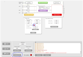
Device Reg Programmer - Cannot detect USB Instrument at address ADC35XX_1 A. Traceback printed below.
Traceback (most recent call last): File "core\instrument\mInstrumentController.py", line 182, in __init__ Error: (2, 'Device not found.') 

Got an error Connecting to hardware. Running in Simulation Mode.
No RegProgrammer defined
Got an error Connecting to hardware. Running in Simulation Mode.
ADC35XX - Device registers reset.
dev, Dummy write : 0 = 1 
dev, Dummy write : 0 = 0 
dev, Dummy write : 8 = 0 
dev, Dummy write : 17 = 0 
dev, Dummy write : 7 = 8 
dev, Dummy write : 7 = 72 
dev, Dummy write : 19 = 1 
dev, Dummy write : 19 = 0 
dev, Dummy write : 7 = 75 
dev, Dummy write : 25 = 2 
dev, Dummy write : 31 = 16 
dev, Dummy write : 31 = 80 
dev, Dummy write : 10 = 8 
dev, Dummy write : 11 = 0 
dev, Dummy write : 12 = 0 
dev, Dummy write : 24 = 16 
dev, Dummy write : 25 = 18 
dev, Dummy write : 32 = 0 
dev, Dummy write : 33 = 252 
dev, Dummy write : 34 = 15 
dev, Dummy write : 25 = 18 
dev, Dummy write : 27 = 128 
dev, Dummy write : 27 = 136 
dev, Dummy write : 36 = 0 
dev, Dummy write : 39 = 0 
dev, Dummy write : 46 = 0 
dev, Dummy write : 39 = 0 
dev, Dummy write : 46 = 0 
dev, Dummy write : 37 = 0 
dev, Dummy write : 42 = 0 
dev, Dummy write : 43 = 0 
dev, Dummy write : 44 = 0 
dev, Dummy write : 45 = 0 
dev, Dummy write : 49 = 0 
dev, Dummy write : 50 = 0 
dev, Dummy write : 51 = 0 
dev, Dummy write : 52 = 0 
dev, Dummy write : 38 = 32 
dev, Dummy write : 38 = 34 
dev, Dummy write : 38 = 2 
dev, Dummy write : 38 = 0 
Error in reading from Reg programmer
dev, Dummy read : 7 = 75
dev, Dummy write : 7 = 75 
dev, Dummy write : 8 = 0 
dev, Dummy write : 17 = 0 
dev, Dummy write : 8 = 0 
dev, Dummy write : 17 = 0 
dev, Dummy write : 7 = 75 
dev, Dummy write : 19 = 1 
dev, Dummy write : 19 = 0 
dev, Dummy write : 7 = 75 
dev, Dummy write : 25 = 18 
dev, Dummy write : 31 = 80 
dev, Dummy write : 10 = 8 
dev, Dummy write : 11 = 0 
dev, Dummy write : 12 = 0 
dev, Dummy write : 24 = 16 
dev, Dummy write : 25 = 18 
dev, Dummy write : 32 = 0 
dev, Dummy write : 33 = 252 
dev, Dummy write : 34 = 15 
dev, Dummy write : 25 = 18 
dev, Dummy write : 27 = 136 
dev, Dummy write : 36 = 0 
dev, Dummy write : 39 = 0 
dev, Dummy write : 46 = 0 
dev, Dummy write : 39 = 0 
dev, Dummy write : 46 = 0 
dev, Dummy write : 37 = 0 
dev, Dummy write : 42 = 0 
dev, Dummy write : 43 = 0 
dev, Dummy write : 44 = 0 
dev, Dummy write : 45 = 0 
dev, Dummy write : 49 = 0 
dev, Dummy write : 50 = 0 
dev, Dummy write : 51 = 0 
dev, Dummy write : 52 = 0 
dev, Dummy write : 38 = 32 
dev, Dummy write : 38 = 34 
dev, Dummy write : 38 = 2 
dev, Dummy write : 38 = 0 
Error in reading from Reg programmer
dev, Dummy read : 7 = 75
dev, Dummy write : 7 = 75 
#================ ERRORS:6, WARNINGS:153 ================#

I attempted to perform the same operations on another computer, to no avail.

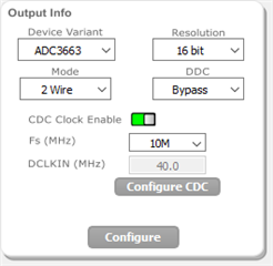
My GUI configuration is the following :


Could you please help me on that topic ?

Thank you.

  • Hello,

    Thank you for sharing the details of this issue.

    If the sample clock is not present when the ADC35XX EVM GUI is launched, then the ADC3663 will not respond to SPI write/read commands, and causes the GUI to not function properly (like the "dummy" writes shown in the log you shared).

    Can you please ensure that the sample clock coming from the onboard clock is present? You can probe the resistors you installed to verify (R41/R51).

    Additionally, please also disconnect/reconnect the mini-USB cable to ensure that the FTDI chip on the ADC3663EVM is not being utilized by another source on your PC (sometimes that can happen unexpectedly).

    Once verified that the clock is present, please close and relaunch the ADC35xxEVM GUI. If all is well, the PLL Lock LED will illuminate after the GUI has launched. You can then select the Fs that you would like to use, and click Configure CDC.

    Now you are ready to capture the ADC3663EVM data with the TSW1400EVM, in accordance with the ADC366xEVM user's guide.

    Best Regards,

    Dan

  • Hi Dan,

    Thank you for your answer, I get no clock when probing the resistors but a DC voltage of ~500 mV on R41 et ~200 mV on R51. Pressing ADC Reset button or connecting / disconnecting the cable does not change.

    Best regards.

  • I probed the quartz Y2 at R59 and I get a clean 10 MHz Sinusoid, but it is clipped in the negative on R55. Is it expected ?

  • Hi Quentin, yes, the XO distortion on one of the outputs (R59) is expected. This app note may help explain Selection and specification of crystals for Texas Instruments ethernet physical

    Please see attached images of our ADC3663EVM that has been modified to successfully use onboard clocking.

    ADC3663EVM Onboard Clock.zip

    Since there is only a DC voltage output on R41/R51, and no PLL lock comes on, it sounds like there is still an issue with the hardwared configuration, or the USB interface.

    The GUI configures the CDCE6214 (Onboard clock) during its initial setup routine, so you should see a 10 MHz signal on R41/R51 without having to do anything beyond launching the GUI.

    Can you please share a picture of your ADC3663EVM and a screenshot of the ADC35XXEVM GUI (right after the GUI has completed its setup)?

    Best Regards,

    Dan

  • Hi Dan,

    I performed the same modifications as you. Please find attached the pictures of the board, as well as the GUI after startup and after attempting to reconnect (CDC switch was set to on but went back to off after the attempt).

    TI_Debug_Pictures.zip

    Thank you.

    Best regards,

    Quentin

  • Hi Quentin,

    Thanks for sharing these images. In terms of hardware configuration, I believe everything looks fine.

    Just to be clear, if you start with the ADC3663EVM USB disconnected and the ADC35XXEVM GUI closed, then connect the ADC3663EVM USB and launch the ADC35XXEVM GUI, the PLL_LOCK LED does not come on at any point?

    Looking at the screenshot you shared (TI_GUI_After), the device variant ADC3663 is present (good), but looks like the GUI is still in simulation mode.

    On the ADC35XXEVM GUI, can you click the "Reconnect USB" button? Also, can you click the "CDC Clock Enable" slider button (currently red)? Does this turn green?

    Best Regards,

    Dan

  • Actually, I set the "CDC Clock Enable" slider to green but it switched back to red as soon as I clicked the "Reconnect USB" button. At no point does the "PLL_LOCK" LED lights up.

  • Hi Quentin,

    Can you please confirm that ~+3.3V is present at the "CDC 3.3V" test point (this is located near the PLL_LOCK LED)?

    After you plug in the ADC3663EVM, but before you launch the ADC35XXEVM GUI, can you please probe resistors R41/R51 with an oscilloscope?

    The PLL_LOCK LED will not be lit at this time, and you should see an non-periodic waveform when probing R41/R51(see attached image). I believe that you said there was only a DC level, but wanted to make sure that this was checked before launching the GUI.

    Best Regards,

    Dan

  • Hi Dan,

    I confirm that there is +3.3V at the test point "CDC 3.3V". ON R41 is still get a pure 260 mV DC and on R51 a pure 570 mV DC.

    I only plugged the board without launching the GUI, and after trying mutiple restarts of the board using the reset switch.

    Best regards.

  • Hi Quentin,

    Thank you for checking. It sounds like there is some issue on the board with the onboard clocking chip. I apologize for the inconvenience, but, rather than continuing the troubleshooting, please return the ADC3663EVM.

    You can send the board back using the TI customer support center. Use the TI Chat Support (see image below) to ensure that the latest instructions for the return process are shared.

    If I might suggest a different part, the ADC3643EVM is a 14 bit version of the same family as the ADC3663EVM, and also has a CMOS output data interface. It only requires on clock input (for the sample clock), so the clock and analog input can be coherent/synchronous with only two signal sources sharing a reference frequency.

    Best Regards,

    Dan

  • Thanks Dan I will then return the board,

    I am checking out the ADC3643EVM but I'm a bit confused as to what the DCLKIN is doing in this case. I can use the same clock signal for both clocks ? Because the exemple in the user guide uses two differents clocks frequencies but there is decimation involved, which should not be part of my application.

    Since I have already tested two different sets of ADC + Data capture boards and have still not achieved the result I am looking for, I am a bit cautious ... I would also rather keep 16 bit depth since my application requires precision, but a typical sampling rate lower than 2 MSPS.

    Best regards.

  • Hi Quentin,

    I understand your trepidation, and my aim is to reduce any additional time lost.

    With the ADC3643EVM, you can use the parallel CMOS interface (no decimation required) that only requires a single clock input (sample clk) for the ADC to output the sampled data. Where the ADC3663EVM requires a sample clk and DCLKIN to output sampled data.

    The ADC3643EVM is also capable of a serial CMOS output, but would then require a sample clk and DCLKIN, just as the ADC3663EVM. This would not be the target usecase, but I'm just mentioning this to address the reason for why DCLKIN is present on the ADC3643.

    In terms of performance, the ADC3643EVM will have about 3 dB less SNR (79 dBFS), but will have lower power consumption (and lower cost).

    By default, the ADC3643EVM utilizes the onboard clocking chip, and you will be able to have a seamless "out-of-box" experience. If you want to utilize external clocking, then some resistor modifications will need to be made (similar to what was done on the ADC3663EVM).

    If you can let me know exactly what you are trying to do, in terms of sample clock and the analog input, I can provide the best part/EVM recommendations.

    Please let me know if you have any additional questions or concers.

    Best Regards,

    Dan

  • Thank you Dan for your answer,
    Could we please talk in private messages so that I can expose you with further details ?
    The application is quite confidential, with pending patents and high risks if I disclose too many informations publicly.