This thread has been locked.

If you have a related question, please click the "Ask a related question" button in the top right corner. The newly created question will be automatically linked to this question.

ADS7038: Trouble reading the analog inputs

Part Number: ADS7038

Hi,

I'm just starting to work with the ADS7038. I'm currently trying to read all 8 inputs using the manual mode, but it looks like the chip just keeps sending the same value from analog 0 and does not advance to read any other analog point.

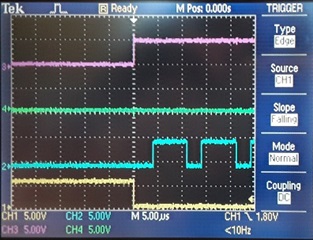
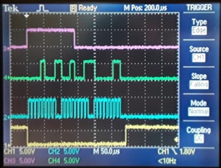
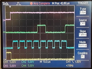
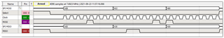
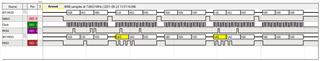
I'm talking to the ADS7038 over the SPI port and I'm confident that the interface is working because I can write to a register and read it back successfully.

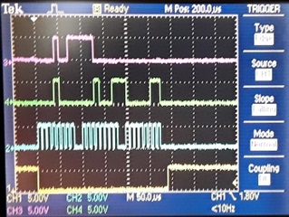
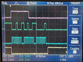
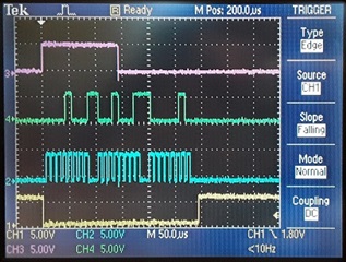
For testing the manual mode, it looks like all of the initial settings (CONV_MODE=00, SEQ_MODE=00, & PIN_CFG=0 from page 23 in the ADS7038 datasheet) are their default values, so I didn't change any of them. Then I gave the ADS7038 these 3 commands to see if I could read the first 3 analog inputs (write to the CHANNEL_SEL register, Address=0x11):

08, 11, 01; set MANUAL_CHID to 1 for the next read

08, 11, 02; set MANUAL_CHID to 2 for the next read

08, 11, 03; set MANUAL_CHID to 3 for the next read

In each case when I look at the data that was received, it looks like it just keeps reading analog 0 as I mentioned above.

Can anyone me what I'm doing wrong and what I can do to fix it?

Thank you for your response.

Brad McMillan

  • Hello, 

    would you please provide a scope shot of the digital communications, including CS, SDI, SDO, and SCLK. Please include 3 SPI frames

    Regards

    Cynthia

  • Hi Cynthia,

    Here it is with CS, SCLK, SDI and SDO bottom-to-top.  Hopefully the resolution is good enough, I just took a picture with my camera.

    Thank you so much for the assistance.

    Brad McMillan

  • Hello Brad, 

    would you please include three consecutive frames, the data for this command will not appear until two frames after. it is fine if these is in three different images

    Also this image is not very clear on timing. Is the t_SU_CSCK timing being met, this is the time from the CS falling edge to the first SCLK capture edge, in this case it would be the first rising edge. This has to be a minimum of 3.5ns. 

    for debugging, i would also suggest using different known DC inputs at each input channel. this will make it easy to know what to expect and what data corresponds to what. Ie ch0=gnd, ch1=1V

    Regards

    Cynthia

  • Hi Cynthia,

    I added a delay between CS and the first SCLK pulse and it is now 4us so that should be more than enough:


    I put the following voltages on the first three inputs: ch0=5v, ch1=0v, and ch2=1v.

    Then I sent the following three commands:

    08, 11, 01; set MANUAL_CHID to 1 for the next read

    08, 11, 02; set MANUAL_CHID to 2 for the next read

    08, 11, 03; set MANUAL_CHID to 3 for the next read

    As you can see, I get the same response each time; 0FFF, which is the full-scale (5v) value on ch0.  The chip never advances to read the next channels.

    Thank you again for your response.,

    Brad McMillan

  • This is rather odd.

    Could you try a could of tests to try to isolate the source

    1.After the first register write command, provide two CS frame with SDI pulled low, essentially two empty frames, I would like to see if the SDO data will be pushed out. 

    2. would you use the FIX_PAT feature of the device, register DATA_CFG (address = 0x2) has an option to set a fixed pattern as the SDO data instead of the measured data. this was included to help with communication issues. Once this is set, the ADC will output a fixed data pattern as the ADC output data. Page 31 of the datasheet has the register content information.

    Is there a 1-µF decoupling capacitor to GND connected to pin 8 of the device?

    Regards

    Cynthia

  • Hi Cynthia,

    I performed the tests but without much luck.  I tried to consolidate the responses so the pictures are pretty small.  I hope they are still readable for you.

    1. Here is the result with SDI pulled low after the first write command:

    It had the same result as before with 0FFF for each frame.

    2. Then I tried setting the FIX_PAT bit in DATA_CFG, but I didn't get the expected pattern:


    3. Then I tried reading the DATA_CFG register after I set the bit and that didn't even work:

    The response was 0xFF and not the expected 0x80.

    Here is the layout:

    There are 3 1uf bypass capacitors for AVDD, DECAP, and DVDD.

    It looks like I might have been mistaken when I thought I was writing to the registers successfully.  I see in the data sheet that there are 4 different SPI protocols.  I haven't done anything to set the SPI protocol.  Do you think that might be the problem?  I'm talking to the ADS7038 with a Zilog eZ80F91 processor and I'm talking to it through opto-isolators.

    Thank you again for your assistance.

    Brad

  • Hi Brad,

    I think you probably identified the root cause.

    The default clocking scheme (SPI-00) in the ADS7038 datasheet shows in figure 8-9 that SDO is available to sample on the rising edge of SCLK. I'm not familiar with the Zilog but default value in the Zilog register SPI_CTL (CPOL = 0 and CPHA = 1) means that your uC is sampling SDO on the falling edge according to Table 111 in the manual.

    So the solution appears to be to reset bit CPHA in register SPI_CTL in the uC at start-up so that the sampling edge is rising and  SCLK idle is low. However that leaves you with the problem that SS will go high between bytes, again according to Table 111. Unfortunately it appears that you can never make a 24-bit read/write register command in order to take control of the ADS7038. It could be that the Zilog SPI is fundamentally incompatible with this ADC out of the box.

    All is not lost however. If all the above is correct, you should consider changing the pin function of SS to a standard GPIO and toggle it manually before and after a 24 bit SPI transaction. If you cannot change the pin function of SS then disconnect it from ADS7038 altogether and substitute it for a standard GPIO which you are able to toggle manually. This manual toggling of SS is the very technique used in the ADS7038 demo code for manual conversions so is a perfectly sound solution from the perspective of the ADS7038.

  • Actually Brad I'm seeing a similar problem.

    The manual channel selection does not appear to work for me either. After a device reset, each individual channel works as expected but then if I move the channel to another MUX input, I just get high ADC values where I should get close to 0.

    So it might not be a Zilog clocking problem in practice or it could be we both have a timing problem or there is something we are both doing wrong in the ADS programming.

    I'll report back if I find a solution.

  • I fixed my issue. The problem was that my AIN inputs we're floating. As soon as I connected them to ground or a test voltage I got reasonable results.

    OK Channel 4 is a bit high but the results seem to eliminate an SPI comms problem.

    I think the cause is that the sample and hold capacitor holds charge from channel N. If channel N+1 is then selected by the MUX but N+1 is floating, the SAH cap does not discharge or charge to a new value so N+1 channel kind of inherits the sample from N.

    Assuming you don't have a comms issue Brad, what are your AIN inputs connected to?

  • Cynthia and Kier,

    Still no luck.  The Zilog eZ80F91 is set for SPI-00 (CPOL=0 & CPHA=0) and the ADS7038 datasheet says that is its default also. 

    SPI-00 specifies that the data is read on the rising edge of SCLK.  I looked at a write register command (0000 1000b) on the scope:

    and it looks good to me; it looks like the "1" is being picked up on the 5th rising edge.  I wrote an 0x80 to address 0x02 so I expected to see the 0xA5A test pattern, but it never showed up.

    Can you guys see anything I'm doing wrong here?

    Thank you for your response.

  • There is a good point here that the analog input should not be left floating. For debugging i suggest using different known DC inputs for different channels, ex Ch0 = gnd, Ch1=1V, and so on. This helps to compare the expected output with the actual output. 

    When using the Fixed pattern, this eliminates this possibility, as the output is now controlled by the device and not the analog input signal. 

    Looking at the latest image you shared, the clock pulses do not look very even, the low time is substantially shorter than the high times. 

    This device  only allows a limit for high and low SCLK time to be from 45%  to 55% of the clock time, your clock does not look to meet this. 

    Regards

    Cynthia

  • Hi Brad,

    Cynthia's point about the asymmetric clock notwithstanding, your scope plot doesn't seem quite right. Yes, the 1 bit is in the right place but why is green trace rising again after the eighth bit and why does the SCLK stop after 8 bits?

    For reference, here's my 0x08 0x02 0x80:

    Note the position of the FIX_PAT is not in the read back data itself but on SDO when SDI = 0x10 (READ_REG).

    Looks like you should try to fix the clock symmetry first as suggested by Cynthia.

  • Hi,

    It's working now (yay!).  I figured that the asymmetry is most likely caused by the opto-isolators and would be less significant at lower frequencies so I slowed it down by a factor of 4 and now everything is working; I can get it to generate the test pattern and I can read the analog inputs beyond ch0.

    BTW Kier, the reason SCLK stops after 8 bits is that I was only showing the first 8-bit SPI frame so I could show a clear picture of the relationship if SDI to SCLK.  There were 2 more 8-bit SPI frames for a total of 24 bits but they weren't shown on the scope.

    Thank you both for the assistance.  I would have never figured out what the problem was without your help.