This thread has been locked.

If you have a related question, please click the "Ask a related question" button in the top right corner. The newly created question will be automatically linked to this question.

DAC81404EVM: Cannot Set DAC Output Registers

Part Number: DAC81404EVM

Hello TI,

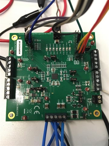
I have DAC81404EVM board along with MSP-EXP432E401 launchpad. But after i cannot get DAC output and i could not be sure whether i can read/write the registers, i switched to ESP32 thanks to @ParswaNath 's library

https://github.com/sphCow/DAC81404_lib/blob/main/main.cpp

When i read the registers i will get the below results : 

0x00 : 0
0x01 : A70
0x02 : 8
0x03 : A86
0x04 : 4000
0x05 : F
0x06 : 0
0x07 : 0
0x08 : 0
0x09 : FFF0
0x0A : 0
0x0B: 0
0x0C : 0
0x0D : 0
0x0E : 0
0x0F : 0
0x10 : 0
0x11 : 0
0x12 : 0
0x13 : 0


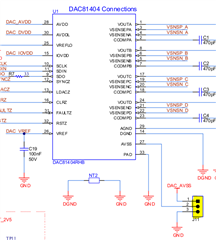
Here you can see internal reference register (0x04) is in false (0x4000) state. When i checked the TP11 it is 0 volt. When i change 0x04 (internal reference register) to true, i could see the 0x04 register is changed to 0x00 and i could see 2.5 volt on TP11. What i understand is that i could write and read register successfully (Am i right ?). Apart from Parswa's library, i changed the SPIMODE0 to SPIMODE2 to read/write register. 

My problem is that i could not set register 0x09 (Power Up Channel), 0x0A (DAC Range) and i could not write DAC value as well. When i try to write 0x09 i could only make channel 0 to power up (0xFFF0) as you can see above but in this condition i could not set DAC Range and DAC value as well for channel 0 (channel 0 is DAC output A, right ?). For other channels i could not make them power up. Could you please help me for this problem.

Best Regards

Fatih

  • Hi Faith,

    The DACPWDWN register (0x09) uses the last 4 bits to power up the channels. 0xFFF0 means that all channels have been powered up (the last 4 bits are all zero). The DACRANGE and DACn-DATA registers are write only meaning you can't read them back. You may have written to them successfully. 

    What are the jumper settings on the EVM?

    Is the CLRZ (J3) jumper open or closed? 

    If the internal reference is powered down, how are you supplying the external reference?

    Best,

    Katlynne Jones

  • Hello Katlynne;

    Here is the picture of my board : 

    You can see the jumpers (It must be its default positions). J3 is in open position.

    The connector below is J17. I connected its 1st pin to 5V. 2nd and 3rd pin to GND. 4th pin to AVDD which is 12 Volt at the moment. and 5th pin to GND.

    When i checked the test pins TP1, TP2 or TP3 i could not see the voltage (0 Volt). I am writing different values to DAC output registers (0x10, 0x11, 0x12, 0x13). 

  • Hi Faith,

    It looks like you have CLR and RST connected to the controller you are using. What is the voltage level of these signals? They should be high or the DAC outputs may be being cleared or a device reset is being triggered.

    Best,

    Katlynne Jones

  • Hello Katlynne;

    CLR and LDAC cables are not connected to my controller. I could connect and change their levels if you want.

    We are using RST at the initial phase of  the code.

     pinMode(_rst_pin, OUTPUT);
     digitalWrite(_rst_pin, LOW);
     delay(1); 
     digitalWrite(_rst_pin, HIGH); 
     delay(1);

    Its latest pin level is HIGH.

  • Hi Faith, 

    If you don't have the CLR and LDAC signals connected then they are pulled up to DAC_IOVDD on the EVM which is fine. You can verify that these signals are high with a meter just to be sure. 

    If the internal reference is powered down, how are you supplying the external reference? It looks like you have J16 open which means the onboard 2.5V reference is not connected to VREF.

    Best,

    Katlynne Jones

  • Hello Katlynne,

    I checked the CLR and LDAC pins. CLR pin is high but LDAC is low which is okay as far as i know according to default Jumper settings. 

    I dont really understand the reference voltage issue could you clearify little bit what should i do ?

    What i have done is that i powered the board through J17 as i mentioned above. I tested the voltage with/without J16 short circuited and with/without internal reference activated via register 0x04. But i could not get any DAC out voltage.

    Best Regards

    Fatih

  • Hello Faith,

    I think you are using own controller for SPI communication. could you please share programming code and  snap of your SPI signals. I want to look sequence.

    Can you able to read and write register correctly ?

  • Hello Anbu,

    Yes i could read and write SPI registers correctly as far as i understand. As i mentioned above, i could read device ID and other registers. More, i could read GENCONFIG (0x04) as 0x4000. When i changed (0x04) and write 0x0000, i could read the register as 0x0000 and when i checked the TP11, i could see 2.5 V which was 0 Volt before changing the register. So, i could change the register 0x04 and i change the voltage reference from external to internal. Furthermore, register DACPWDWN (0x09) is starting as 0xFFFF and i could change it to 0xFFF0 by enabling channels. What it means i write and read to the registers.

    As a programming code, i utilizes ParswaNath's library https://github.com/sphCow/DAC81404_lib/blob/main/main.cpp . Only difference is that i changed SPI mode from SPIMODE0 to SPIMODE2. I could snap SPI related parts for sure.

    #define DAC_CS 5
    #define DAC_RST 22
    #define DAC_LDAC 12
    #define DAC_CLR 14
    
    DAC81404 dac(DAC_CS, DAC_RST, DAC_LDAC, &SPI, 30000000);

    int res = dac.init();
    dac.set_int_reference(false);

     dac.set_ch_enabled(0, true);
      dac.set_ch_enabled(1, true);
      dac.set_ch_enabled(2, true);
      dac.set_ch_enabled(3, true);

    dac.set_range(0, DAC81404::U_10); //   0 -> +10V
      dac.set_range(1, DAC81404::U_10);  //  -5 -> +5V
      dac.set_range(2, DAC81404::U_10);  //   0 -> +6V
      dac.set_range(3, DAC81404::U_10); // -10 -> +10V

    dac.set_out(0, (i)%65535 );
      delayMicroseconds(5);
      dac.set_out(1, (2*i)%65535 );
      delayMicroseconds(5);
      dac.set_out(2, (3*i)%65535 );
      delayMicroseconds(5);
      dac.set_out(3, (4*i)%65535);
    

    Sorry for the code snaps. I could not copy and paste whole code into one code snap. I always get the error : 

    Access Denied
    You don't have permission to access "">e2e.ti.com/.../configure on this server.
    Reference #18.82a0de52.1634014275.28ee01c2

    For SPI or dac init parts, you can check the Parswa's library. I try to copy and paste here but it look very bad due to error above. I only changed the SPI mode from Parswa's library.

    By the way, we could not get the DAC output when we use launchpad as well. I could get the same readings from SPI. Is there a hardware related problem on our board ? How could we check it ?

    Best Regards

    Fatih

  • Hi Faith,

    It looks like the original library has the DAC data registers being written to in a loop:

    uint16_t i = 0;
    bool done = true;
    
    void loop() {
      dac.set_out(0, (i)%65535 );
      dac.set_out(1, (2*i)%65535 );
      dac.set_out(2, (3*i)%65535 );
      dac.set_out(3, (4*i)%65535);
    
      i = (i+64)%65535;  
      delayMicroseconds(1);
    
      
      /*
      if(millis()>10000 && done) {
        dac.set_ch_enabled(2, false);
        Serial.println("ch 2 shutdown");
        for(int i=0; i<4; i++) Serial.printf("ch %d power -> %d\n", i, dac.get_ch_enabled(i));
        Serial.println();
        done = false;
      } */
    
    }

    What is your value for i in the code snippet you shared? 

    Thank you,

    Katlynne Jones

  • Hello Katlynne,

    Yes it is the same code you shared which is in the library, My code is also running in the loop. I could not share the code like you did because of the error Access Denied.

    Best Regards

    Fatih

  • Hi Faith, 

    Can we simplify the code to just set one DAC output to full scale (0xFFFF) instead of writing in the loop. Make sure the internal reference is enabled via register 0x04 and jumper J16 is open to disconnect the external reference. Set the SPICONFIG register (0x03) to 0, and disable the read functions in the code. Set the DACPWDWN register (0x09) to 0xFFF0. 

    It will also be helpful if you can send an oscilloscope shot of the SPI frame. I believe SPIMODE 2 is correct, but I recently ran into an issue where someone had the device in the wrong mode and was still able to set the internal reference on and off, but was not able to update the DAC outputs. It will be helpful to verify that the SPI is working correctly.

    Can you also try removing J2 to pull the LDAC pin high? 

    Are you applying an external IOVDD external to J20? What is the position of jumper J19? 

    Thank you,

    Katlynne Jones 

  • Hello Katlynne,

    I simplified the coed with : 

      dac.write_reg(0x03, 0x0000);
      dac.write_reg(0x04, 0x0000);
      dac.write_reg(0x09, 0xFFF0);
      dac.write_reg(0x0A, 0x1111);
    
      dac.write_reg(0x10, 0xFFFF);
      dac.write_reg(0x11, 0xFFFF);
      dac.write_reg(0x12, 0xFFFF);
      dac.write_reg(0x13, 0xFFFF);

    When i do that i could get 3.8 V on DAC output. And if i do code below in loop : 

      dac.write_reg(0x10, 0xFFFF);
      dac.write_reg(0x11, 0xFFFF);
      dac.write_reg(0x12, 0xFFFF);
      dac.write_reg(0x13, 0xFFFF);
    
      delay(1000);
    
      dac.write_reg(0x10, 0x0);
      dac.write_reg(0x11, 0x0);
      dac.write_reg(0x12, 0x0);
      dac.write_reg(0x13, 0x0);
    
      delay(1000);

    I could see that voltage output change between 3.8 V and 0 Volt constantly.

    If i change the internal reference to external reference by writing 0x4000 to 0x04 register and plug the Jumper to J16 i could get the same result constantly changing from 3.8 Volt to 0 Volt (i am providing 12 V to 4th pin of J17 (AVDD)). 

    However if i try to write the DAC output value (0x10,0x11,0x12,0x13) other than 0xFFFF and 0x0000 i could not get any voltage output from DAC output. At startup i change the DAC output value to 0xFFFF and i could get 3.8 V output. Then i change register value to 0x1000, then DAC output value goes to 0 V.  After that i try to change it to 0xFFFF again but i could not get any voltage output anymore 0 V.

    I dont provide external IOVDD through J20, jumper position of J19 is default (2-3). You can check the jumper status from picture above.

    Plugging or removing J2 jumper does not change the situtation.

    I try to get the oscilloscope shot of the SPI frame but before that i want to tell the latest situation so you may get some clues from these results.

    Best Regards

    Fatih

  • Hello again Katlynne,

    I added the SPI frames as i said above comment.

    The code i used is : 

    dac.write_reg(0x03, 0x0000);
      dac.write_reg(0x04, 0x0000);
      dac.write_reg(0x09, 0xFFF0);
      dac.write_reg(0x0A, 0x1111);
    
      dac.write_reg(0x10, 0xFFFF);
      dac.write_reg(0x11, 0xFFFF);
      dac.write_reg(0x12, 0xFFFF);
      dac.write_reg(0x13, 0xFFFF);

    I got the SPI frame of writing DAC output registers (0x10, 0x11, 0x12, 0x13) value 0xFFFF 

    Channel 1 : CS

    Channel 2 : SDO

    Channel 3 : SDIN

    Channel 4 : CLK

    First picture is frame of writing 4 dac output registers. (0x10, 0x11, 0x12, 0x13)

    Second picture is frame of writing 2 dac output registers (0x10, 0x11)

    Third picture is frame of writing single DAC output (0x10)

    I hope it helps.

    Best Regards

    Fatih

  • Hi Faith,

    It doesn't look like the complete SPI frame has been captured. I don't see the full 24bit clock on channel 4.

    It seems like you might not be meeting the SPI timing requirements. The data in line stays high when you write 0xFFFF, so if you aren't meeting the timing requirements some of the '1' bits might be getting captured and some might be getting skipped and that is why you are seeing 3.8V. Can you try slowing down the clock speed to see if that helps? 

    If you have an oscilloscope that can capture the entire SPI clock and a time scale so we can verify the timings then that will be helpful. If you do, Try capturing a write of 0xFFFF and 0xAAAA. 0xAAAA will let us see the data in line toggling bits.

    Thank you,

    Katlynne Jones

  • Hello Katlynne,

    I checked the SPI clock frequency and saw that there is one 0 more (I set 30 Mhz instead of 3 Mhz). Sorry for silly mistake :(  When i decrease it i could see the 24 bit clock.

    I have one more issue about DAC output range. After i set voltage ref to external (writing 0x4000 to 0x04), when i set dac output voltage to 0x0000 i could get 0 V, 0x1111 i could get 0.66 V and 0x5555 i could get 3.33 V. But when i set 0xAAAA or 0xFFFF i get 3.93 V. After setting hex 0xA6FE (decimal 42750) i always get the same result. I could not get more than 3.93 Volt. I set the DAC range to 0-10 V (writing 0x1111 to 0x0A) and shortcircuited J16. I supply 12 V to AVDD (J17 pin 4) and GND for pin 5.

    When i change the voltage reference to internal (writing 0x0000 to 0x04) result is the same. When i change the J11 position from 2-3 to 1-2 i could get 6.53 V for 0xAAAA and 0xFFFF.  After setting hex 0xA6FE (decimal 42750) i always get the same result. I could not get more than 6.53 Volt. 

    Here is the SPI frame for 0xAAAA to 0x10 : 

    I think there is a misconfiguration about registers or jumpers but i am not sure.

    Best Regards

    Fatih

  • Hi Faith,

    The max SPI SCLK frequency is 50MHz with an IOVDD of 3.3V. But for now let's try getting the full 10V range with the 3MHz SCLK. Thank you for the scope shot, the SPI mode looks correct. In an earlier response you mentioned you had J17 pin 1 connected to 5V, 2nd and 3rd pin to GND, 4th pin to AVDD (12V), and 5th pin to GND. The 5th pin is AVSS, so the position of J11 shouldn't have mattered. The options for J11 are AVSS (which you had connected to ground), or GND. 

    It seems like the jumper settings are correct. And the register settings seem correct. Up to 0xA6FE (6.53 V) we see the correct voltage levels. This seems like a headroom issue.

    Do you have any load on the DAC channel output? Or are you just measuring with the scope? If there is a large load the headroom requirements increase:

    And what type of supply is the 12V AVDD? 

    If possible, can you measure the current through the output and AVDD as you increase the DAC code, and make sure the 12V supply remains at 12V as you increase the DAC code.

    Another test could be to increase the AVDD and keep the range the same. If there is a headroom issue, then increasing AVDD should let you see greater than 6.53V.

    Best,

    Katlynne Jones

  • Hello Katlynne,

    We found the problem. It was a grounding issue. We use Channel 1 to supply EVM and Channel 2 for AVDD. When we connect their grounds, we can read correct DAC output values. Thanks for your great support and patience.

  • Hi Faith,

    Great to hear! Please let me know if you run into any more trouble. 

    Best,

    Katlynne Jones