- Ask a related questionWhat is a related question?A related question is a question created from another question. When the related question is created, it will be automatically linked to the original question.
This thread has been locked.
If you have a related question, please click the "Ask a related question" button in the top right corner. The newly created question will be automatically linked to this question.
Hello,
I used TSW54J60EVM (to evaluate ADS54J60) and with Xilinx demo board with JESD204IP. I have obtained valid ADC data with the correct PLL/JESD settings. The sample rate is 983.04MHz, frame mode is 8224 and the sysRef divider is 768.
However, I have difficulties to get the corrector ADC word order. In the FPGA side, for each analog channel, there are 8 words: gt0[31:0] to gt3[31:0] for channel A, and gt4[31:0] to gt7[31:0]. For each channel, there are 8 16-bit words. What is the sequence of these 8 words ? Are there any registers on ADS54J60 that define the sequence ? For example, is A3[31:16] earlier than A3[15:0] ? And is A2[15:0] earlier than A1[15:0] ? Without the correct ADC word sequence, for a sine waveform, I got a sine waveform with saw-shape in each 8 words.
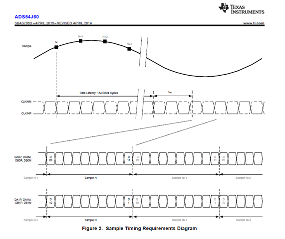
From the ADS54J60 datasheet, I found Figure 2 showing the N sample, N+1 sample. But it doesn't show which lane (DA0 or DA1) has a earlier sample.
The second question is the byte order within a 16-bit word, I don't know how to control it and observed random byte order. For example, for A3, the corrector byte order can be A3[31:16] and A3[15:0]. For for the same frame, A2 byte order is A2[23:16, 31:24] and A2[7:0, 15:8]. I tried to use "Flip ADC data" in the GUI, but it seems doesn't have the fully control of the byte order in one 16-bit word.
Thanks in advance for any suggestions.
-Yuke

Sampling figure in ADS54J60 datasheet

Table 11 in ADS54J60

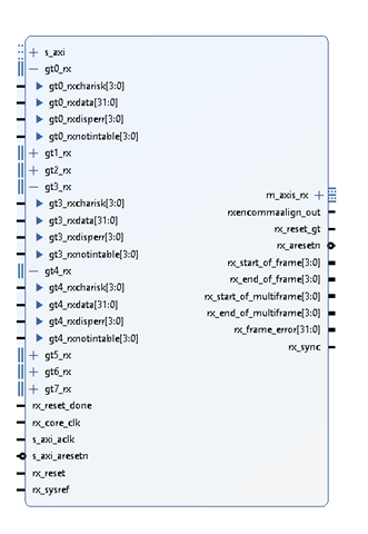
JESD204B on Xilinx Side
Yuke,
The data for CHA is as follows:
First sample is on lane DA2. There are two octets per frame. The first octet is bits 15:8 and the second octet is bits 7:0.
The second sample is on lane DA3. There are two octets per frame. The first octet is bits 15:8 and the second octet is bits 7:0.
The third sample is on lane DA1 and the fourth sample is on lane DA2.
This order then repeats. The same sequence works for CHB but using lanes DB0-DB3.
The Flip ADC data will have the first octet as bits 0:7 and the second octet as bits 8:15.
I am not familiar with how Xilinx handles the data but this is how it comes out of the ADC.
Regards,
Jim