This thread has been locked.

If you have a related question, please click the "Ask a related question" button in the top right corner. The newly created question will be automatically linked to this question.

ADS54J60: Upper bits of lower byte inverted

Part Number: ADS54J60

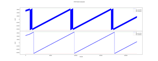
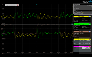
Randomly the chip will either stream data correctly or have the upper bits of the lower byte inverted. Resetting JESD re-randomizes whether or not the issue occurs. On a bad run, the upper 2 bits will randomly become inverted. I believe bit 5 also gets inverted but I'm not 100% sure since the noise floor make it difficult to tell.

Other observations:

  • The issue happens on i and q independently
  • Using the register to swap the JESD lanes used by LSB and MSB result in the issue following the lane that is now sending the LSB (issue follows the data not the JESD lane)
  • Enabling fast OVR results in the lowest byte always being 0 (expected)
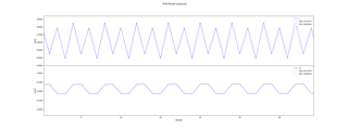
  • Digital gain of non-zero will affect the DC offset and noise floor but will never result in the noise from the inverted bits entering the MSB (which implies the bit flips are occurring after digital gain)
  • Setting a digital gain of 0 results in all data being 0 (which implies the bit flips occur before the digital gain, contradicting the previous point)
  • Roughly half the samples in a bad run will be normal, the other have will be affected by this issue
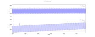
  • About a 1/4 chance of this occurring every time JESD is reset

We are using a board we designed. Previous versions of our board did not have this issue, but we can't find any differences in the state of the ADC between this board in the previous ones.

  • Doug,

    Do you issue a hard reset to the ADC after the clocks are present but before programming the registers?

    Is the JESD link stable when you see this issue? Can you place the ADC in ramp mode to verify the FPGA is capturing data properly when in a bad state? This can be done by writing a 0x40 to address 0xF74 in the ADC Page (Analog Bank Page SEL = 0Fh). The ramp is no ideal since this part has 4 internal interleaved ADC's but it might help with this testing.

    Does your board provide power sequencing per the data sheets? Can you send your register settings?

    Regards,

    Jim

    ADS54J60_test_pattern_ramp_mode CHA_CHB.pptx

  • Do you issue a hard reset to the ADC after the clocks are present but before programming the registers?

    We perform a hard reset by toggling the pin 48 with clocks present.

    Is the JESD link stable when you see this issue? Can you place the ADC in ramp mode to verify the FPGA is capturing data properly when in a bad state? This can be done by writing a 0x40 to address 0xF74 in the ADC Page (Analog Bank Page SEL = 0Fh). The ramp is no ideal since this part has 4 internal interleaved ADC's but it might help with this testing.

    JESD reports no errors on the FPGA side while running. In ramped mode each interleaved core individually looks almost fine but there are 2 issues;

    On I the phase difference between ADC cores on the ramp is significantly larger than on Q.

    On Q about every 500 samples there will be 2 samples ~45 samples apart that are ~300 above the other nearby samples

    Images below (in order) are of 2 full cycles of the ramp, a zoomed in section of the plot to show how Q's cores are a lot closer together than I, and another plot showing the spikes on Q

    2 full cycles of a rampZoomed in section of ramp to show phase difference between interleaved coresSection of ramp plot to show spikes on Q

    Register settings:

    ADS54J60 : regdump
    Master Page Regs:
    0x20: 0x00
    0x21: 0x00
    0x23: 0x00
    0x24: 0x00
    0x26: 0x00
    0x4f: 0x00
    0x53: 0x00
    0x54: 0x30
    0x55: 0x00
    0x59: 0x20
    ADC Page Regs:
    0x40: 0x00
    0x5f: 0xe3
    Main Digital Page Regs: (Channel A       Channel B)
    0x00: 0x00      0x00
    0x41: 0x00      0x00
    0x42: 0x00      0x00
    0x43: 0x00      0x00
    0x44: 0x00      0x00
    0x4b: 0x00      0x00
    0x4d: 0x00      0x00
    0x4e: 0x00      0x00
    0x52: 0x00      0x00
    0x72: 0x00      0x00
    0xab: 0x00      0x00
    0xad: 0x00      0x00
    0xf7: 0x00      0x00
    JESD Digital Page Regs: (Channel A       Channel B)
    0x00: 0x80      0x80
    0x01: 0x04      0x04
    0x02: 0x00      0x00
    0x03: 0x00      0x00
    0x05: 0x00      0x00
    0x06: 0x1f      0x1f
    0x07: 0x09      0x09
    0x16: 0x00      0x00
    0x31: 0x00      0x00
    0x32: 0x00      0x00
    JESD Analog Page Regs: (Channel A        Channel B)
    0x12: 0x3e      0x3e
    0x13: 0x3c      0x3c
    0x14: 0x3c      0x3c
    0x15: 0x3c      0x3c
    0x16: 0x02      0x02
    0x17: 0x00      0x00
    0x1a: 0x00      0x00
    0x1b: 0x80      0x80
    Offset Read Page Regs: ()
    0x68: 0x82      0x82
    0x69: 0x00      0x00
    0x74: 0xff      0xff
    0x75: 0x06      0x06
    0x76: 0xe5      0xe5
    0x77: 0x06      0x06
    0x78: 0xfd      0xfd
    0x79: 0x01      0x01
    0x7a: 0x1f      0x1f
    0x7b: 0x01      0x01
    Offset Write Page Regs: ()
    0x00: 0x00      0x00
    0x04: 0x00      0x00
    0x08: 0x00      0x00
    0x0c: 0x00      0x00
    0x01: 0x00      0x00
    0x05: 0x00      0x00
    0x09: 0x00      0x00
    0x0d: 0x00      0x00

    Also it is likely that the entire lower byte is flipped on a bad run during normal streaming, but only the upper 2 bits are known to flip for certain. I assumed the lower bits were not flipped earlier because the FOVR flag would always sent correctly, but since it appears the issue happens much earlier in the chain the fact that the flag always gets through does no indicate that the lower bits are fine when there is regular data.

  • Doug,

    Please add the new register writes I added in red in the attached document. These resets are required as the hard reset does not set all internal registers. In the Main Digital Page, the registers do not get loaded unless address 0x00 bit 0 is toggled from a "1" to a "0". This should always be done at the end of writing to this page.

    Regards,

    Jim

    General Register.docx

  • I added the soft reset register writes to the startup sequence in addition to the hard reset already there, and it seems to have had no effect on the issue. Toggling bit 0 of register 0x00 is already implemented during the reset sequence  All registers in the main digital page should be 0, unless there is something in the data sheet I missed. Manually setting the registers (plus toggling bit 0 of 0x00) for FOVR has the expected result, and setting the digital gain mostly has the expected result so I'm confident reads and writes to the main digital page are working correctly, including the writes done as part of the startup sequence.

    To make it easier to understand what's happening. Here are 2 plots with no input connected. The left is noise (expected), on the right I is just noise but Q has the lower byte randomly inverted.

    Normal outputByte flips on Q

  • Doug,

    I am guessing the left plot is the upper bytes of I and Q and the right plot is the lower bytes of I and Q, correct?

    Is this issue with just one part on one board? Does this only occur with no input? 

    Did the ramp pattern ever show any sign of this? What is the ADC sample rate?

    There is one more register you can try. In the JESD Analog Page, toggle bit 6 of address 0x17. This will reset the PLL (See Table 75 of the data sheet).

    Regards,

    Jim

  • Are there any subsystems that are reset when JESD is reset by asserting the SYNC pin? And is there a way to reset them without bringing down JESD? Ramp gets through on bad runs with less than 1% of the samples wrong (more details below) but in normal mode about 50% of samples are affected. We know that this issue is re-randomized by resetting JESD, but also that JESD is sending the data with very (if any) bit errors.

    I am guessing the left plot is the upper bytes of I and Q and the right plot is the lower bytes of I and Q, correct?

    Correct, I is the top line in each plot and Q is the lower plot

    Is this issue with just one part on one board? Does this only occur with no input? 

    This issue occurs on every board within this revision. It was working on previous revisions of our board. The only 2 changes that may be relevant are switching from AC to DC coupled sysref (to fix a different issue that resulted in I and Q having the wrong phase difference) and a possible reduction in signal integrity. I don't think this caused by signal integrity since the ramp looked fine. The issue occurs both with no input and with input, since the upper byte is working perfectly a strong input signal will look good, other than the imperfections caused by the issues in the lower byte.

    Did the ramp pattern ever show any sign of this?

    The only apparent difference in ramp mode between good and bad runs is that on bad runs Q will have will have 2 single samples spikes ~45 samples apart every 500 samples and I will have 2 samples ~30 samples apart be very slightly off every ~310 samples. The incorrect points on Q are more consistent than I. Less than 1% of the samples in ramp mode are off in a bad run, compared to ~50% of samples in normal streaming. One other note is that in both good and bad runs the ramp jumps every ~2000 samples.

    What is the ADC sample rate?

    1Gsps, LMFS = 4211

    There is one more register you can try. In the JESD Analog Page, toggle bit 6 of address 0x17. This will reset the PLL (See Table 75 of the data sheet).

    I don't know if resetting JESD PLL does anything, since resetting it brings down JESD, which requires resetting JESD on the FPGA side to bring back up, which I already know re-randomizes the issue. Is there a way to check if the internal PLL is locked?

  • Doug,

    There is no way to monitor if the PLL is locked. Can you tell me why you are masking the SYSREF when writing to address 0x54 data 0x30 in Master Regs page? Can you remove this and see if this helps. SYSREF is required to reset internal state machines. Is there a chance SYSREF is not getting sampled properly since you switched from AC to DC coupling? Is the SYSREF common mode voltage (1.3V) and amplitude (0.35 - 1.4V diff) at the correct levels?

    Regards,

    Jim 

  • Sysref has a common mode voltage of 1.25V in our system and a differential amplitude of 0.37V

    We mask sysref because we used to have an issue where JESD would go down then come back up if we had sysref in continuous mode, and masking sysref after bringing up JESD fixed the issue. Switching back to having sysref always be unmasked now doesn't have any effect. Presumably the instability was fixed when we switched from AC to DC coupling. Normally our system will unmask sysref before resetting JESD, however it I leave sysref masked and manually reset JESD there does not seem to be a difference

    Also about the switch from AC to DC coupling; originally this hardware revision had AC coupling, however we modified them to have DC coupling to fix an issue where I and Q would have random phase differences (between each other, from the same ADS54J60). This byte flip issue was present both before and after the modification.

  • Doug,

    Not sure how changing SYSREF from AC to DC coupling could possibly fix the phase issue you were seeing. There should not have been any phase issue as both internal ADC's use the same SYSREF input.

    Can you try the attached procedure and see how this works?  Follow it exactly as is if possible. This is the procedure we use with the TI EVM. By default the SPI will write to both channels so you should only need the writes I have provided. We will not test with the OVR setting for now. Just want to focus on the byte swap issue.

    Regards,

    Jim

    General Register 4211.docx


  • Performing those exact steps doesn't seem to make any difference compared to before.

    What is the allowable common mode voltage range? The datasheet says 1.3V without specifying a maximum or minimum. Currently the common mode voltage in our system is 1.25V

  • Doug,

    I am checking with the design team regarding this. Is there a way to increase the CM and/or the amplitude to see if this helps? Your diff swing is very close to the minimum.

    Regards,

    Jim 

  • I have not been able to make the modification to the common mode voltage/amplitude yet, but I have found more info.

    The problem is not from a byte flip, but instead because the upper and lower bytes are out of sync. It looked like a byte flip because in much of my testing I had either no or an extremely weak signal connected, and having the lower byte from a positive sample, mixed with the upper byte of a negative sample looked like a byte flip. In a good run with the ramped test mode anytime the upper byte increments the lower byte rolls over in the same sample. In a bad run 1 of 2 things will happen:

    1. The lower byte will roll over in the sample after the sample where the upper byte increments

    or

    2. The lower byte will increment extremely slowly (at a similar but no identical rate to the upper byte)

    It is possible to have I and Q independently fail in different ways.

    We used to have an issue where I and Q were out of sync and that was fixed by changing sysref from AC coupling to DC coupling. It seems the current issue is caused by the upper and lower part of the byte being out of sync

  • Doug,

    I would suggest trying different values for the elastic buffer delay (RBD) in your FPGA JESD IP Core. You may also want to increase the K value as well to allow for more lane buffering. The buffer release point in your FPGA may have been right on the boarder, which is why you see this issue randomly.

    Regards,

    Jim