This thread has been locked.

If you have a related question, please click the "Ask a related question" button in the top right corner. The newly created question will be automatically linked to this question.

ADS54J60: Stuck bits in received data

Part Number: ADS54J60
Other Parts Discussed in Thread: , STRIKE, ADS54J20


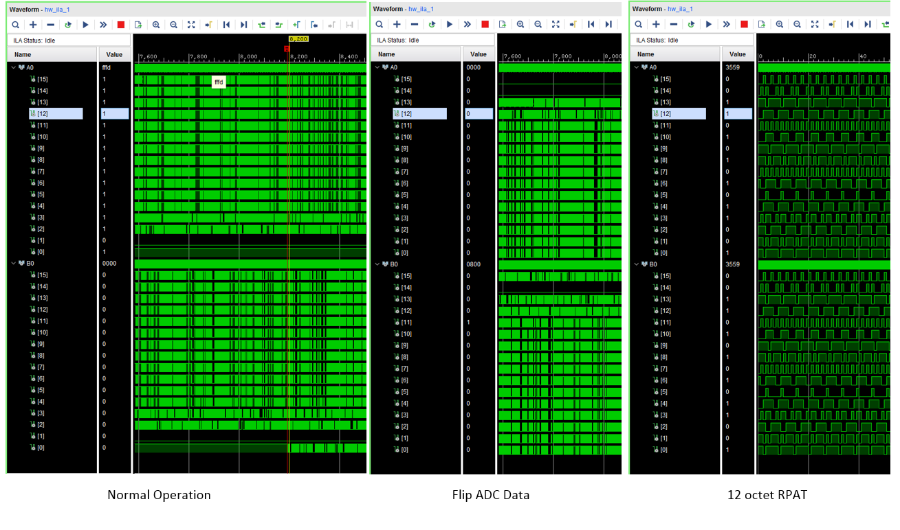
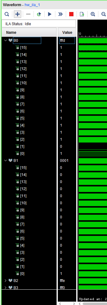
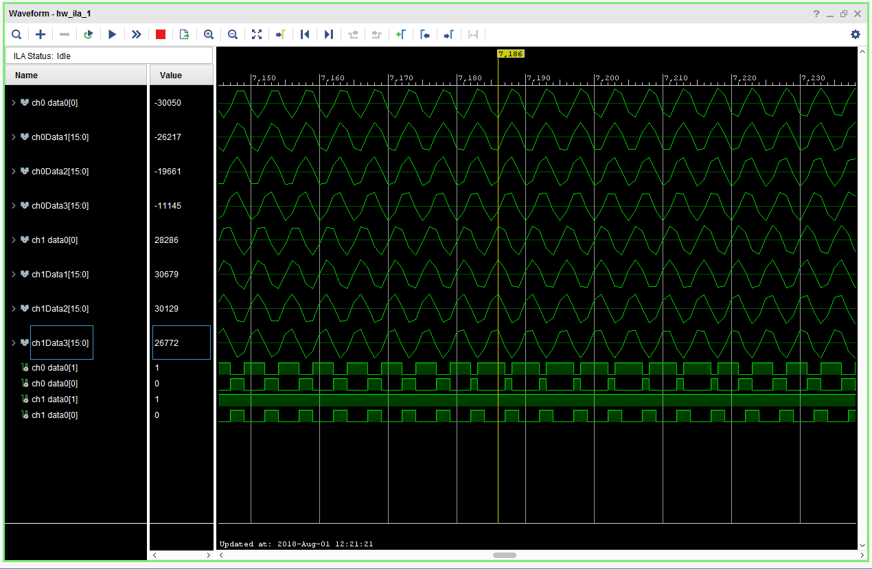
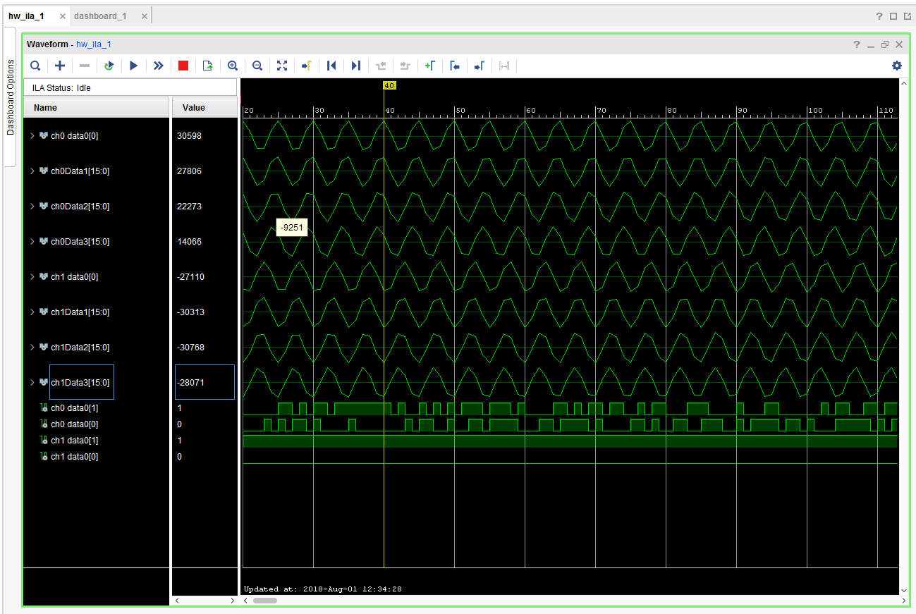
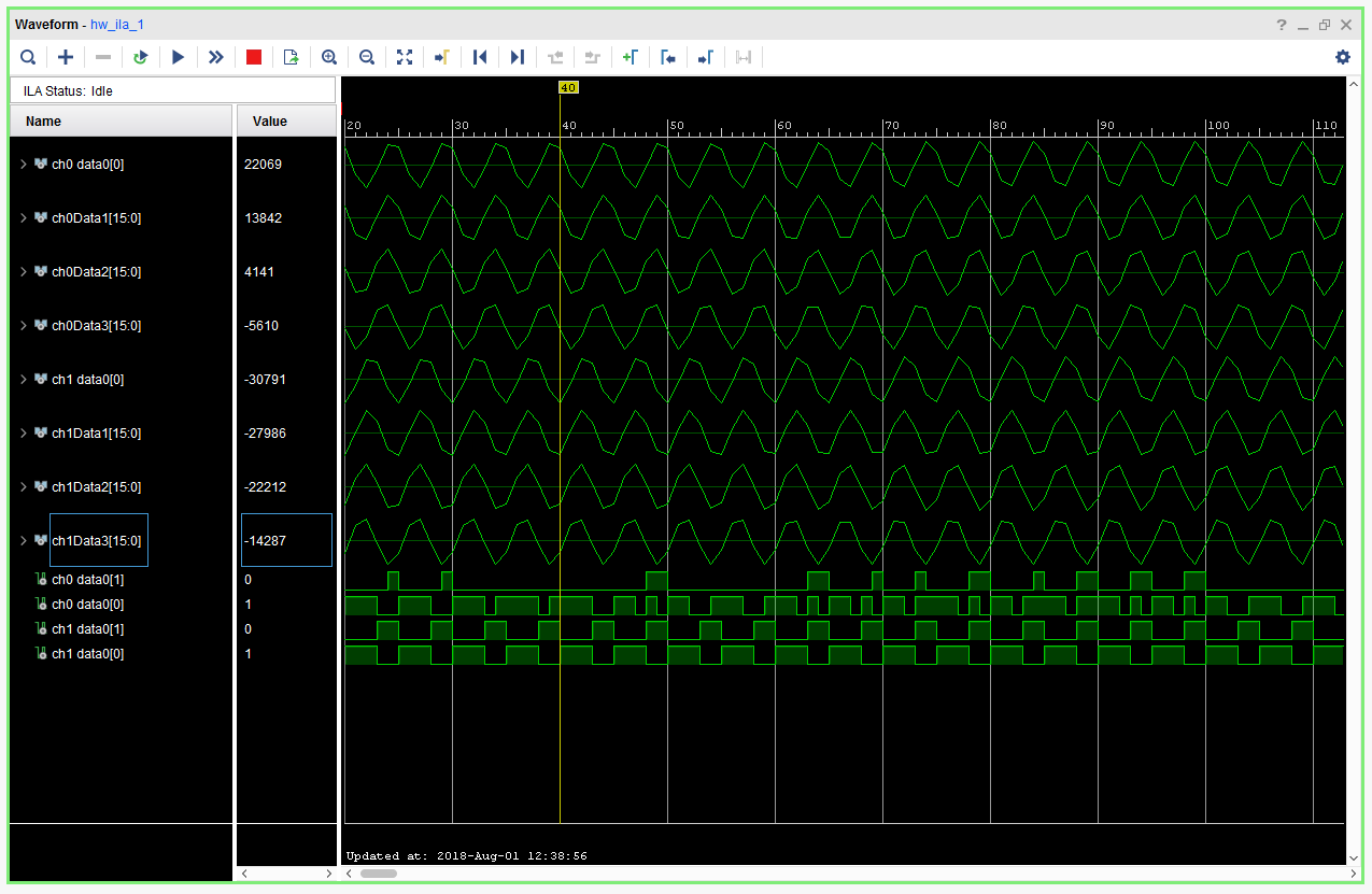
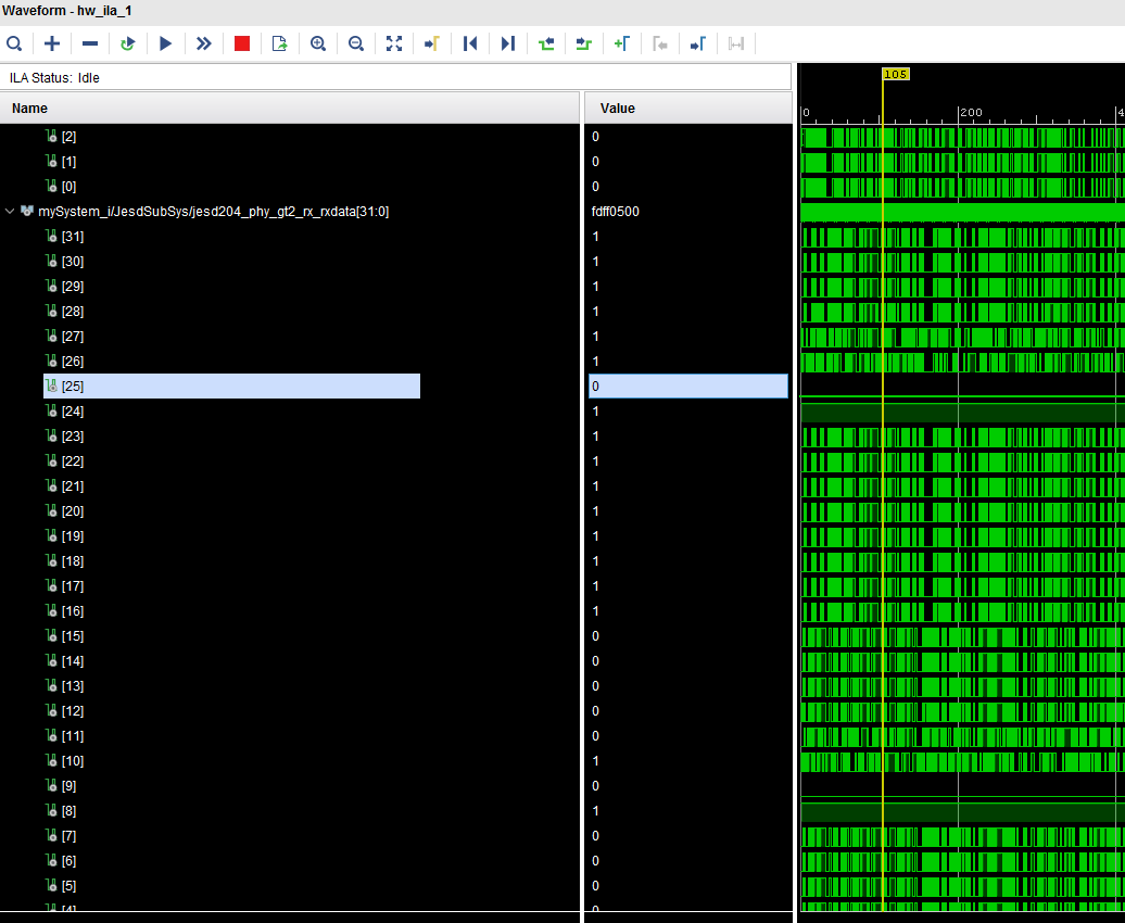
In the following setup we are seeing some stuck bits in position A0(1:0) and B0(1:0) in the received ADC data on the FPGA.
Sometimes bit 0 toggles in the data, sometimes it is stuck. But bit 1 is always stuck.

IF we "Flip ADC Data" then the position of the stuck bit changes to A0(14:15) and B0(14:15)

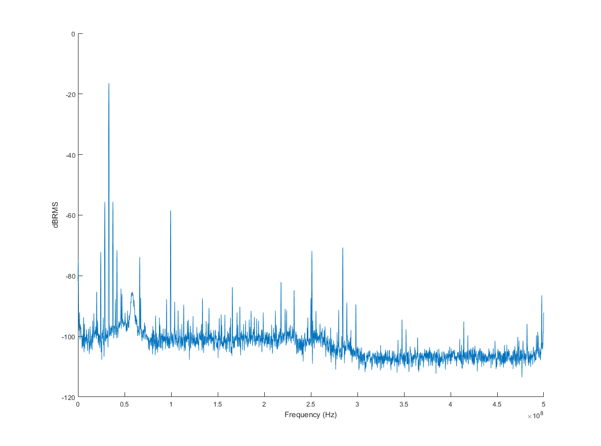
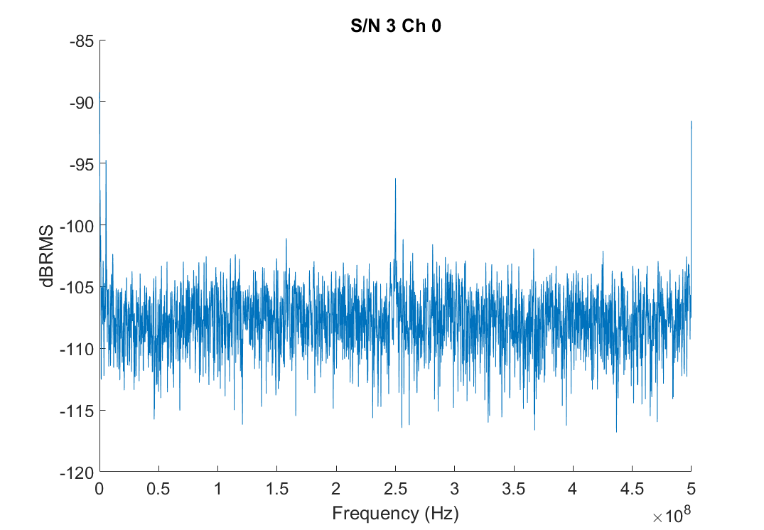
If we us the 12 octet RPAT JESD Test pattern there are no stuck bits.

(diagram below shows captures from 3 scenarios)


We observe the same in our custom board based on the below setup.

Setup:

ADS54J60EVM connected to Xilnx KCU105
External 1GHz clock used

FPGA clock = 250MHz
K = 16
SYSREF Divider set to 256
SYSREF in continuous mode

The steps we follow are:

Program the FPGA
Load a modified version of LMK_Config_External_Clock to generate the requried clock & sysref frequencies
Press the ADCReset button
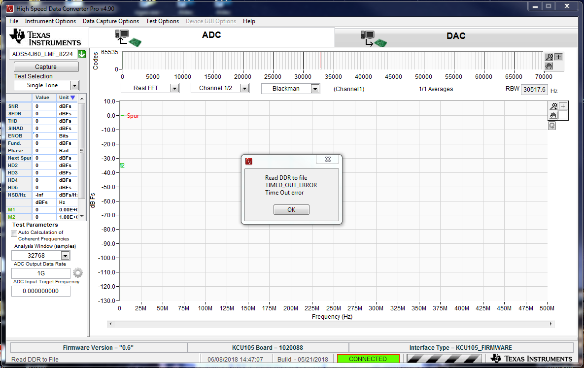
Load ADS54J60_LMF_8224.cfg
I have alo tried a modified version of this file to remove the LMK writes to assert and deassert the sysref (as we want it in continuous) however this makes no difference.


Can you suggest any problems in our setup which would cause this problem?

Kind regards

  • Isabel,

    Can you try using the ADC in 4211 and 4244 mode to see if this has any different results? Does slowing down the sample rate change anything? Is SYNC stable? What is the frequency of SYSREF? You just mention a divided by 256. Is the LMK providing the 1GHz clock to the ADC or is this from some other source? If it is from another source, it must be synchronized with LMK. I have a KCU105 and can try and duplicate this test as well. I just need this information so my setup is just like yours.

    What version is the ADC GUI you are using?

    Regards,

    Jim 

  • Hi Isabel
    We have received your question. Someone will provide a more detailed response soon.
    Best regards,
    Jim B
  • Hi Jim, Thank you for the quick reply.

    I will try the 4211 and 4244 modes, and slowing down the sampling rate change.

    I assume you are referring to the SYNC signal into the ADC? We've probed it and it is stable and high.

    The SYSREF frequency is 3.90625MHz (1000/256).

    The LMK is providing the 1GHz ADC clock.

    The JESD core is setup to 'Drive JESD204 core clock using global clock', and the LMK is configured to generate a 125MHz core clock on CLKout 12.

    We are using ADS54Jxx GUI v1.8.

    Just to clarify my original post - which may have been confusing.  My screen shot only showed the two channels of ADC data which had stuck bits.Samples A1, A2, A3, B1, B2 & B3 are all ok (see B1 below) i.e it is just every 4th sample of ADC data at 1GHz which has stuck bits.

    Kind regards, 

    Isabel

  • Isabel,

    When I looked at the earlier screen shots, it appears like thousands of consecutive samples are having issues with the two bits, not just every fourth sample.

    Regards,

    Jim
  • In the screen shots the only bit to not be toggling is A0(1) and B0(1), B0(0) will some times be static and some times toggle. Given this is noise all the other bits are just sign bits. And just to be clear by every forth sample that means every A0 sample. The Vivado ILA is running at 250MHz, for the full giga sample pattern will have A0,A1,A2 & A3 at 250 MHz. The same applies to the other channel.

    Richard

  • Richard and Isabel,

    Can you do an eye scan (IBERT) on the FPGA serdes inputs? I would be interested to see how the lanes that are connected to FMC pins B16/B17 and A6/A7 compare to the other ones. These are the lanes that contain only A0 samples and B0 samples. If you are able to run the other LMF settings, this will place other samples on the same lane as A0 and B0. If there is an issue with the lane, I would then expect you to see bad data from the other samples as well.

    Regards,

    Jim

  • As Isabel said in her first post we experience the exact same thing with our custom FPGA board where the ADCs, LMK and FPGA are on the same PCB. The same happens on both of the custom boards we've tried. This combined with it producing the same behavior on the KCU105 makes me believe it's not a hardware problem.

    We've been trying to debug the issue using the KCU105 as it gives us more direct access to the LMK and ADC registers but so far no combination has cleared up the issue.

    I'm trying to workout what effect this stuck bit will actually have on our data as overall the data looks fine although capturing the data from the ILA an running spectrum analysis on it does show some content at 250 MHz which could be a manifestation of the slight bias the stuck bit causes on every 4th sample.

    Richard
  • I have just tried to use the build that comes with the High Speed Data Converter Pro following the instructions in slau711. When required to change the FMC VADJ to 1.8V, when doing the Read FMC HPC is says the card is not present. Regardless of this I tried to continue setting up the LMK and ADC for a 1GHz reference although the instructions are not for the ADS54J60EVM so the menus in the guide don't match. I then try a data capture and get a timed out error.

    Is the reading the FMC an issue or not given we've got a different board from the guide. Are you able to provide a configuration file for the LMK and ADC that will definitely work for a 1GHz reference in distribution mode.

    The other thing I noticed in the instructions was about connecting the clock to two inputs, J5 and J7. I guess this is the equivalent of J4 and J6 on our board. Given we want to use the LMK in distribution mode is there a need to provide both clocks?

    Cheers

    Richard
  • Richard,

    Connect an external 1GHz source to SMA J6. Go to the low level view tab and navigate to the file called "LMK_Config_External_Clock.cfg". This will setup the LMK for clock distribution mode. After loading this file, press the board ADC reset switch then load the "ADS54J60_LMF_8224.cfg" file. This will get the ADC EVM up and running. This will provide a 250MHz clock to the FPGA. The SYSREF default divider value will be 768. You may want to change this to 256 under the SYSREF and SYNC tab on the GUI.

    What revision is the ADC EVM you have? Can you send me the labeling info on the ADC part itself? if you think this may be caused by the ADC, I  am willing to send you a replacement board. If so, I would like to get your board to see if we can duplicate your issue with our capture board.

    Regards,

    Jim


  • Using those two scripts I can't get the HSDC Pro software to capture the data. That LMK script doesn't have clock 12 activated so I assume the JESD core in your design is setup to use a single clock. It'd be nice to get your HSDC Pro build working so are those scripts you pointed me at definitely designed to work with the bit file provided with that software? The first capture I tried I get an error message about the JESD core, all other captures then say DDR timeout.

    Also you never answered my question about being able to adjust the VADJ and not being able to read the FMC EEPROM section of the SLAU711 instructions. 

    As we've said previously we see this stuck bit behavior on both ADCs that are on our own FPGA cards so it's unlikely to be the individual devices. 


  • We checked the hardware and there is an appropriate delay between those rails so the mod has been done on the EVM. On our hardware we use the first rail to enable the second rail rather than using a capacitor but this also has the desired effect.

    Whilst on the phone I forgot to remind you of Isabel's point in the first post that when using the test pattern the bits toggle ok, demonstrating it isn't an issue with that lane.

    The problem occurs when the ADC is sampling real data and forming it into the JESD transport layer.
  • I also had another go with the HSDC Pro build with the window set to 32768 (in both places) but still get the DDR timeout error. Are you able to send me the capture you did with your setup as a file of some sort.

  • Richard,

    I just received this from the design team:

    "By default OVR of one of the four interleaving cores is placed at bit[1] of 16 bit output data instead of ADC’s data. This is a bug.

    However, this bug doesn’t change overall performance since last two LSBs are buried under thermal noise of ADC.


    This ‘Always write 1’ bit corrects the bug by removing the OVR and placing ADC’s data on bit[1].


    From customer’s description it appears that this may be the reason why he sees bit[1] stuck in every 4th output sample.

    Let’s see if his problem persists even after setting this bit."

    To fix this you need to always write a "1" to bit 1 of address 0x12 in page 0x6A00

    Regards,

    Jim

  • Adding more "chipscope" to the noddy design I shared with you I am able to see that the static bits are present in the data stream coming out of the phy section of the JESD core. I believe phy has nothing to do with sysref or sync but just undoes the 8b10b encoding so this really does suggest the static bit is in the transmitted data.

    We've also used the example design created with the JESD IP and also see the stuck bits.

    As I've said though given we see this on a range of hardware I don't believe it's a hardware fault (although I guess if you can send me some 1G sample data with an 8224 JESD scheme to show it's not a general problem) but probably the way we're driving or setting up the device.
  • Please try this register write change.

  • Register address 0x12 in page 0x6A00 doesn't show up in the low level view of the GUI.
    We added the following line to the ADS54J60_LMF_8224.cfg file

    0x6A0012 0x02

    Looking at the register map we couldn't see a way to select which channel (A or B) this applies to .
    Is there anything else we need to add to the cfg file?


    Kind regards
  • 0602.ADS54J60_LMF_8224_new.cfgIsabel,

    If you add it to the config file, it will automatically write it to both channels.

    Regards,

    Jim

  • Just to reply to the comment about those bits being in the thermal noise. Bellow is the current ADC noise floor we get (this is done by capturing from our design in Vivado and importing into matlab as I am unable to get the HSDC Proc build to work). As you can see there is a distinct tone at 250MHz.

  • That was the change we tried but the resulting behavior is not consistent.
    On successive ILA captures
    - Sometimes both bits [1] and [0] of A0 and B0 toggle
    - Sometimes all of them are stuck
    - Sometimes 1 or 2 of them toggle and the others are stuck. There seems to be no pattern to it.

    The behaviour certainly has changed by writing to that address. Previously, bit [1] did not toggle at all. But it hasn't fixed the problem.

    Regards, Isabel
  • Isabel,

    Thanks for the info. Is there anyway you can send us time domain data? This may help the designers trouble shoot this issue.

    Regards,

    Jim

  • What time domain data do you want? Attached is a CSV file of the data without writing to that register.

    I have been under the impression that the stuck bits were causing the 250MHz tone, if in fact another issue is causing that then that is my priority. When used in our system we will have carriers at 210MHz and 310MHz so do not want extra tones around that area.

    iladata.zip

  • Here's a screen shot of the behavior after the register write when inputting a 2Vpp 50MHz signal. The offending bits from channels 0 and 1 have been replicated at the bottom. They are now toggling (although occasionally you can get a capture with them back to static) but the pattern suggests they aren't random, especially since on ch0 bit 1 is the inverse to bit 0. 


  • Here's some more captures I'm not sure what makes it transition from one pattern to the others.


  • Even when I occasionally get a capture with what looks like random toggling the 250MHz tone is still there. Here I've got a 33MHz single which has some harmonics from the sig gen but images are also created either side of the 250. Have you got some data you've captured or your system that shows if the setup is correct we can get a better spectrum.

  • Richard,

    Attached is data I captured with our EVM using an external 1GHz clock and 210MHz and 310MHz inputs. I do not see much of a spur around 250MHz. I also captured data with no input and one of the IF tones backed off to -10dBm. The .csv file we wanted was with the new register setting applied with a typical analog input you plan on using.

    Regards,

    Jim

    ADS54J60_Ext_1G_210_IF.pptx

  • Your signal generator is obviously cleaner than ours. It would be nice to get the HSDC Pro working on our setup if you could tell me how to get passed that DDR timeout error. I see you had the capture window at 65536 so I guess it doesn't need to be reduced to 32768.

    I'm surprised not see anything at 250MHz as your own data sheets says there should be interleaving tones there but I guess you sig gen has raised the noise floor enough to cover it.

    Have you de-interleaved the capture to see if every 4th sample has stuck (or atleast odd) behavior in bits 0 and 1. If you're able to achieve that spectrum with the bits being weird then it means they're not important and it's another setup issue that's creating the 250MHz.

    Attached is the data the plots are from. I have an input signal at 1MHz, 33MHz and 50MHz. I didn't use our actual frequencies as the extra noise from our sig gen would end up masking the problem tones. 

    0640.ilaData.zip

  • 4745.ADS54J60_LMF_8224_new.cfgLMK_EXT_CLK_KCU105.cfgADS54J60_KCU105.pptxRichard,

    See if these files and instructions can get you up and running with the KCU105.

    Regards,

    Jim

  • Still get this message

  • Richard,

    Could you try this using the ADC with the on board clock source? You would use the file called "LMK_Config_Onboard_983p04_MSPS". If this works, there may be an issue with your external clock source.

    Regards,

    Jim 

  • I'll give this a try but don't forget I have had data successfully captured on my KCU105 build albeit with the stuck bits. The problem with the HSDC build seems to be nothing to do with the ADCs.
  • We're starting to run out time to keep going round in circles so it'd be useful to just get to the bottom of these issues. Bellow is the noise floor we currently get from our real hardware, the 10 dBRMS for the interleaving tone seems inline with the data sheet even though your capture did seem to be better. This is still with the the LSBs on A0 and B0 doing funny things. 

    Have you concluded that the bits are a fundamental characteristic of your ADC? Where you able to de-interleave your data to see if you are also having that issue?

  • Richard,

    Sorry for the delay. I am expecting a new chipscope project today from our firmware team and still waiting to hear back from the design team regarding this. Does your plot above look exactly the same before and after you do the new register write info we sent you? What input (frequency and amplitude) are you sending the ADC in the capture above? I would like to duplicate this setup exactly the way your are doing it. Is your external clock filtered? What amplitude is this? There is chance you may be able to reduce this spur by disabling the DC offset correction feature and sending your own correction values. Attached is a document explaining on how to do this. This is something that will be added to the next revision of the data sheet.

    Regards,

    Jim

    7658.ADS54J60_DC_CORR_External.pdf   


  • This is our raw ADC noise floor, no signal is being injected. The ADCs will be driven from the output of balanced optical detectors and our calculations suggest that the ADC will be the limiting factor even if we're getting the full 11.6 ENOB which is why we're checking the noisefloor is as expected.

    The 1GHz clock souse is an RFX OS364 part. It currently just free runs but in the full system will be trimmed to a GPS 1PPS. The circuitry mimics that of the eval board.
  • I should add this was without the extra register write. In our main system the clock distribution and ADCs are setup by a processor and we haven't updated it's source to set the extra register.

    I was comparing the latest config files you sent with mine. One big differences is the ADC stuff at the end of the LMK script. Is this necessary given the procedure is to reset the ADC via toggling the hardware line before running the ADC script which also resets things with the registers. As for other differences your unused outputs have slightly different settings but I guess as long as they're powered down it shouldn't make any difference. Two things that did strike me as odd, you have clkIn1Mux (reg 0x147) set to PLL1 where we set it to Fin and you have the PLL2 charge pump (0x169) disabled but we had it on tri-state.
  • Richard,

    We have duplicated this setup and using chipscope, show no sign of this issue. Is this still an issue?

    Regards,

    Jim

  • We definitely still see those stuck bits even after that extra register write. If you can send us your bit file, ltx file and config files then we can see if we can get our setup to do the same as yours.

  • Lanerate_4p9152G.zipRichard,

    The files are attached. This was used with Vivado 2016.1.

    Regards,

    Jim


  • I assume I'm meant to use the config files you sent previously to setup the clocks and ADC. If I do thiat and then program the FPGA I get LED4 flashing fast with all the others off. If I do a capture in chipscope everything comes back zeros.

    Is there a button on the devkit I need to press to engage some reset logic to establish the link?

  • Richard,
    Are you still needing help with this?
    Regards,
    Jim
  • Yes, as I said above I can't get that devkit build you created working

  • Richard,

    Try downloading this source code from the link below and run the command set TARGET "TI" before creating the project to generate a TI bitstream that will work with HSDC Pro GUI. This was created with Vivado 2016.3.

    Regards,

    Jim

    https://txn.box.com/s/plwkmtitzfk223bm7ine4js66n3wis2s

  • 1200.KCU105 HSDC Pro User's Guide.pdfRichard,

    Can you follow the attached document and follow section 7.4 but use the ADC config file with "ADS54J60" in the name instead of "ADS54J20"? I was able to run this with our ADS54J60EVM and showed no signs of stuck bits. Once you have a valid capture, on the HSDC Pro GUI, select bits mode to display all of output bits from the ADC. This setup uses the onboard clocking circuit so no external clocks are required for this test. 

    Regards,

    Jim


  • So i'm giving up on trying to get that build you sent me with chipscope from working? Every time I've tried anything with the HSDC Pro build it always comes up with that buffer error i've mentioned a few times above.


  • Richard,

    What version of Vivado are you using? I will see if our firmware team can compile the chipscope project with this version. You did not modify the  ADC EVM, correct?

    Regards,

    Jim

  • Richard,

    What was the issue you were having with the chipscope project we sent? Does it need to be created from another version of Vivado for you to use?

    Regards,

    Jim

  • Hi Jim,

    I have just actually been able to get the bitstream for the chipscope project you sent working.
    I had to program the KCU105 after configuring the LMK and ADC. The procedure I did was as follows.

    Power up both boards
    Load config : LMK_Config_External_Clock.cfg (original)
    Change SYSREF divided to 256
    Press reset button on board
    Load config : ADS54J60_LMF_8224_new.cfg (the one you provided us with,with the new register write)
    Program FPGA with bitfile in Lanerate_4p9152G

    I have done this a few times now. Most times I do not see any stuck bits ... but the most recent time I did. I have attached a screen shot showing the stuck bits. 

    Also, The times where initially there were no stuck bits, if I reprogrammed the FPGA (without doing anything else) on occasion I did also see some stuck bits. These were not always in the same location. One time they were at bits gt2_rx_rxdata 17&16.

    Could I check with you exactly which procedure you were doing, which configuration files you used, and if possible the settings you used for the JESD core?  

    Many thanks, 

    Isabel

  • Isabel,

    One of the attached files show the registers used by the ADC and the other shows the JESD parameters used by the FPGA.

    Regards,

    Jim

     7762.ADS54J60_LMF_8224_new.cfghttps://e2e.ti.com/cfs-file/__key/communityserver-discussions-components-files/73/1121.ADS54J60_5F00_LMF_5F00_8224.ini

  • Thanks Jim,

    Could you confirm I was using the correct cfg file for the LMK also, and that I was performing the operations in the correct order.

    I was actually looking for the JESD core settings used within the xilinx IP interface (eg the .xci for the core) . It was just to compare with our settings to see if we were doing anything significantly different.

    Isabel
  • Isabel,

    I have taken screenshots of the Xilinx IP settings we used in chip scope project and they are in the attached document. 

    A point to note is we took the KCU105 Reference design and recompiled it for ADS54J60 LMF 8224, lane rate 4.9152G by changing the Base and PHY IP settings with signals added in chip scope. There is no change in the custom logic except for the IP change. So you can refer KCU105 Reference design to understand how the IP clock and resets are handled.

    Regards,

    Jim

    IP settings.zip