This thread has been locked.

If you have a related question, please click the "Ask a related question" button in the top right corner. The newly created question will be automatically linked to this question.

ADS1281: ADS1281PWR

Part Number: ADS1281

Hi,

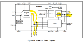
Catalog Number - ADS1281PWR.

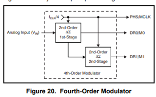
I can't use SPI communication lines so I connect the M0 and M1 Inputs ports to the FPGA.
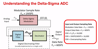
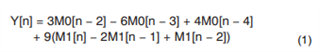
Within the FPGA I compute the Y[n] function and get results in the range of -24 to +25.

When I only used input M0, I knew how to correctly calculate the analog value at the ADC input.

But now, I do not know how to "correctly" treat the values I get from Y[n]. Do I have to constantly sum up the last 32 results of Y[n]?

Thanks.

  • Hello Amir,

    By your response, I'm assuming you are using MOD = 1 so that DRx/Mx are used as modulator outputs. If you are not then SPI is the only accessible way get "data".

    As a result, I am assuming that if you cannot use the SPI lines then your intent is to use M0 and M1 as modulator outputs, not inputs. 

    As a reminder, the output of modulator is a pulse code modulated (PCM) signal, which is a signal where the density of 1's will represent the value of the signal. You can think of it as a array of values that represents a voltage. A very high level info explanation can be found here: https://training.ti.com/ti-precision-labs-sar-delta-sigma-basic-operation?context=1139747-1140267-1128375-1147914-1147913 (around 8 minutes). Mostly, designers will apply a digital filter and decimator to covert from the PCM to a singular code to represent a voltage. So if you do not have those blocks set up in your FPGA, then you should implement them.

    Note, this is the benefit of using SPI because the ADS1281 will filter the signal and provide an easy to read output of signal of interest. I can also guarantee that implementing FPGA code for a digital filter stage will be much more difficult that implementing a GPIO stage for SPI. So, if you have no come up with strict criteria for the FPGA filter stage (which is why designers enjoy the ADS1281), I suggest you reconsider your current plan.

    That all being said, M0 and M1 are both outputs of the modulator where M0 controls the one 2nd order stage and M1 is another 2nd order stage to create a 4th order modulator in series. Lower order stages trade off low latency for higher noise. If you don't have a preference, I suggest you use M1.

    Specifically, Y[n] is an array of signed integers, representing the modulator's quantization level, where "n" represents the array index. The equation is from the datasheet. There is also a paragraph on some more intuitive understanding of the modulator output (VIN = +FS means 90% density of 1s, etc). If you do use M0, all of the M1 parts of the equation will disappear and the index n, will shift accordingly.

    Best,

    -Cole

    Edit: I forgot to add the calculator, here it is

    6813.ADS128x Bitstream.xlsx

    Please refer to this post if you want to learn more about it: https://e2e.ti.com/support/data-converters-group/data-converters/f/data-converters-forum/892895/ads1281-ads1281-pcm-encode-spec 

  • Hello Cole,

    thank you for your response!

    First question, with respect to the Excel file you attached, do I need to perform at least an average of 197 results of Y [n]? If not, what is your recommendation?

    Second question, if we take the sample of 197 samples as an example, should I provide a result that indicates the voltage at each MClk pulse?
    Refers to a first result whose average is the sample range M0 and M1 from sample number 1 to 200 and then the second result is sample number 2 to 201.
    or
    Need to get a result in each new sample set? For example a first result is based on samples 1 to 200 and a second result is based on samples 201 to 400.

    Best,

    Amir

  • Hello Amir,

    Averaging and the PCM signal is a pretty dependent subject from my understanding. What I mean by this, you must average and filter the PCM to get something useful. There is a modulator noise profile in the datasheet which will kill the SNR spec if you do not filter and average to get rid of it. So whether you do use a moving average or decide to designate and array of 197 or 19700 to average is up to you. 

    I'm sure you're familiar with the averaging theorem that says you will decrease the noise by 1/sqrt(n) where n = number of averages. So if you're just trying to verify the value you're putting on the input to ensure you're getting the right data, then average after running it for a reasonable amount of time (e.g. a minute of a few) so that your noise isn't affecting the raw signal you're supposed to be getting.

    For a real system, you're trading off latency for a lower noise result, and I cannot give you guidance what your system needs. Putting the device into a known state, setting an averaging criteria and doing some statistical analysis on those results, might help you achieve your goal.

    I'm sorry I couldn't give you something more concrete. 

    Best,

    -Cole