This thread has been locked.

If you have a related question, please click the "Ask a related question" button in the top right corner. The newly created question will be automatically linked to this question.

ADS1294: What are the correct voltages and configurations to read ECG signals

Part Number: ADS1294
Other Parts Discussed in Thread: ADS1298ECGFE-PDK

Hello,

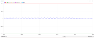
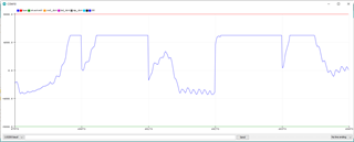
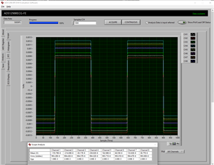
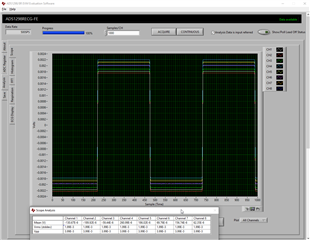
I am using ADS1294 and trying to measure signal from Channel 2. I am not sure if I am configuring the registers of ADS 1294 correctly. I am able to read and write data to the registers correctly. I am also not sure if the voltages of my supply and other pins are correct.

My voltages at different pins are as follows:

Avdd: 2.45V

Avss: -2.6V

Vrefp: 0 // My question is it suppose to be 0 V or +2.5V?

Vrefn: -2.6V // I can configure this to set it to -2.5V depending on my LDO feedback resistor

Vcap1: -1.38V

Vcap2: 0V

Vcap3 = 4.3V

Vcap4 = -1.4V

DVDD: 2.5V // I can configure it to ~1.8V if needed

My register configuration are:

ID:(0x90);
Config1:(0x86)
Config2:(0x00)
Config3:(0xC0) 
Loff:(0x00)
Ch1:(0x81)
Ch2(0x00)
Ch3:(0x81)
Ch4(0x81)

Please note these are the same registers configuration read from ADS chip over SPI communication. 

Procedure which I follow in my code to get the data:

1) on start up I reset it by sensing 0x06 command

2) Then I write the registers by first sending SDATAC command (0x11)

3) Then I send WREN command (0x40) & (0X08), to start writing register from address 0x00 and total register written is 9 hence second byte will be 0x08

4) I then send START command (0x08) after some interval

5) Then RDATAC command (0x10)

6) Make CS high

7) Wait till DRDY becomes low and if low then make CS low and read all the data which is in my case 15 bytes 

Questions:

1) my major concern is the voltages. Is it okay if Vrefp is 0V and DVDD is 2.5V. I missed out 1.8V supply in my design hence applying 2.5V to DVDD with current limiting resistors to limit it to max 3mA..

2) To read ECG signals are the register configurations correct. I am not trying to measure internal test signal.

Thanks,  

  • Hi Gaurav,

    Thanks for the post. 

    All the measured voltages and the register configurations on the devices are correct. The device operating voltage for DVDD is from 1.65V to 3.6V, so DVDD of 2.5V is fine.

    Thanks

    -TC

  • Is it normal that I am seeing signal cutting off and becoming flat in both directions (saturating) while taking EMG even when the Gain is set to 1. Would someone be able to look into my sample snapshot and comment about that behavior. 

    I am not sure if it is because of my code or hardware or something else.

    I have attached sample snapshot as well as code snippet to show how I am converting HEX data from ADS1294 to double data type.

    Resting Baseline Signal:

    Saturated Signal at Gain 1:

    Code:

            long SPI_out_CH2= ((((long)SPI_out_array[k][6]<<24) | ((long)SPI_out_array[k][7]<<8) |((long)SPI_out_array[k][8]<<8))>>8) ; 
    
            double voltage = ((5.0/1)/8388607.0)*SPI_out_CH2*1000;// multiply by 1000 to get voltages in mV

  • Hi Gaurav,

    Thanks for the test information.

    The signal should not be saturated and cut off. I suggest using the internal test signal to verify the signal chain to isolate any issues with the software or hardware.

    Thanks

    -TC

  • I saw a square wave going full range i.e. -2.5 to +2.5 V. What should be the ideal test signal. Can you share screenshot of that.

  • Hi Gaurav,

    The internal test signal should be ±1mV or ±2mV depending on the TEST_AMP setting (CONFIG2.Bit2). Please refer to the FAQ on the E2E for how to convert the ADC output codes to voltage.

    [FAQ] ADS129x: How do I convert ADC output codes to volts?

    Thanks

    -TC

  • I am not reading the exact test signal voltages. I am getting following data:

    • for 1mV test signal with CONFIG2 as (0x10) & CH2SET as (0x05), I am getting (0x1F52) or   0.000398258 V as positive peak of square test signal and for negative peak (0xFFFAEA) or -0.000064671 V. So peak to peak amplitude of 0.000462929 V.

    • for 2mV test signal with CONFIG2 as (0x14) & CH2SET as (0x05), I am getting (0x216B) or  0.000424932 V as positive peak of square test signal and for negative peak (0xFFECD8) or -0.000243584 V. So peak to peak amplitude of 0.000668516 V.
  • As mentioned above the test signal was measured with Vref=2.5, Gain=6. So the LSB based on the link you shared will be 4.9670540273420429632291970588285e-8. Can you crosscheck the values and suggest me solution to fix the issue in order to read 1mV signal accurately.

  • Hi Gaurav,

    The calculation from the ADC output codes is fine. However, the test signal amplitudes from the data capture seem to be incorrect. Please refer to the waveforms below for the internal test signal captured using the ADS1298ECGFE-PDK EVM for both test signal amplitude of +/-1mV (2mVpp) and +/-2mV (4mVpp) using the PGA = 6 setting.

    For debugging, set the input to normal electrode and PGA=1, apply a know DC value at the channel input (INxP/INxN). For this test, you should be able to sweep the channel input from -2.5V to +2.5V based on the design Vref of 2.5V. Please also verify that you are getting the correct reference voltage of 2.5V by measuring the voltage across the VREFP and VREFN pins.

    Thanks

    -TC

  • As mentioned in my first post in this chain my voltages are still same. Can you confirm if VrefP should be 0V or +2.5V.

    My voltages at different pins are as follows:

    Avdd: 2.45V

    Avss: -2.6V

    Vrefp: 0 // My question is it suppose to be 0 V or +2.5V?

    Vrefn: -2.6V // I can configure this to set it to -2.5V depending on my LDO feedback resistor

    Vcap1: -1.38V

    Vcap2: 0V

    Vcap3 = 4.3V

    Vcap4 = -1.4V

    DVDD: 2.5V // 

  • Hi Gaurav,

    For bipolar supply applications, the VREFP should be close to 0V with respect to the ground if you are using the internal 2.4V reference. Therefore, the VREF for the ADC is VREFP- VREFN or 2.6V for your measurement.

    Thanks

    -TC

  • Hi, I was able to verify my internal signals and external signals through a function generator. Everything on benchtop setup works fine. Upon doing a quick EMG signal analysis I found that most of my signals are due to motion artifact. I used a high pass filter of cutoff frequency 15Hz in my calculation to remove out the noise. After doing that my signal looks very weak. I am seeing around +/- 0.1mV EMG signal. I am using Gain of 12 at 250SPS. Please recommend if there is any better way to amplify the signal peaks. I think what I am seeing is combined effects of internal digital decimation filter, notch filter etc. What do you think?


  • Hi Gaurav,

    It is good to know you are able to capture useful data for analysis. Unfortunately, we are not the experts in the EMG application, so the help we can offer is limited. Please note that the internal sinc decimation filter has some rolloff in the passband. You can refer to Figure 52 and Figure 53 in the datasheet, which shows the rolloff characteristic of the sinc filter. As the maximum gain setting of the device is 12, you are limited to using the device in a higher gain setting to amplify the signals.

    As I understand, the EMG signal's amplitude lies between 1-10mV and most dominant in between 50-150Hz. The EEG amplitude from your analysis is significantly smaller than the attenuation caused by the decimation sinc filter. I suspect there may be some other factors that you are seeing such small EMG signals.

    Thanks

    -TC

  • I implemented a software filter using Tfilter online tool to get coefficients/taps for my filter and then I did FIR to get desired signal.