


Hi Tom,
I think I have the same issue of connecting ADS1298-FE Evaluation Board with external microcontroller and
using single supply to the board (AVDD and DVDD) at 3.3V, internal oscillator.
The following is what I have done referring to the previous post :
- J4.5 connects to GND (AVDD)
- J4.9 connects to 3.3V (AVSS)
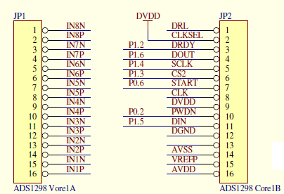
- Jumper JP2 and JP24 open
- Middle pin JP2 connects to 3.3V (DVDD)
- Middle pin J24 GND (DGND)
-JP22 and JP27 open (internal oscillator)
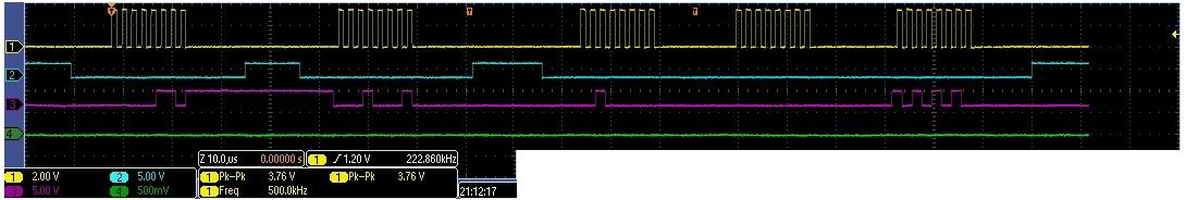
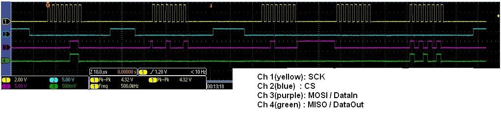
-CS (J3.1) for SPI chip select, JP25 set to make sure J3.1 connect to SPI_CS
-START( J3.14) connect to output port microcontroller set to high; J26 set make sure J3.14 connect to SPI_START
-DRDY (J3.15) connect to input microcontroller
-DIN (J3.11) connect to microcontroller SPI_DOUT
-DIOUT (J3.13) connect to microcontroller SPI_IN
-JP5 (PWDN) is open
I could not read the register so far. I there anything wrong with my hardware connection before looking further for firmware ?
Thank you very much.
Best Regards,
Bunfai


