This thread has been locked.

If you have a related question, please click the "Ask a related question" button in the top right corner. The newly created question will be automatically linked to this question.

ADS42JB69: DC Coupled LMH6554 Driver?

Part Number: ADS42JB69
Other Parts Discussed in Thread: LMH6554, ADC3664, ADS62P44, ADS62P43, ADC16DV160

Hello,

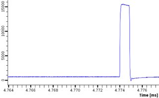
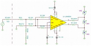
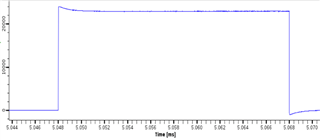
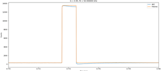
We purchased a DC-coupled, single-ended ADC card with a ADS42JB69 ADC that is being driven by a LMH6554.  The ADC driver circuit follows the typical application schematic on the LMH6554 datasheet, minus the AC coupling caps.  When we apply a square pulse we get droop on the top of the pulse and undershoot when the pulse ends, as if something is AC coupled.  Can the ADC be driven in this DC-coupled configuration?

Thanks,

Trent


  • Trent,

    See if the attached app note helps with this issue. Make sure the common mode voltage is correct at the ADC input. What does the input look like at the7128.app note.pdf ADC input pins?

    Regards,

    Jim


  • Hi Jim,

    Thanks for the app note.  We are seeing a droop on the top of the pulse (it ramps downward) that I do not see in the time-domain figures in the app note.  If the gain=0.95 path is straight through then I would not expect that to happen.  Is there an DC block inside the ADC?  Is the LMH6554 driving circuit appropriate for this ADC?

    Thanks,

    Trent


  • Trent,

    This device has a buffered input but it has a capacitance component to it. See description below from the data sheet. Can you try adding series resistors per the comments below to see if this helps? I would also suggest posting this to the high speed amplifier forum to get their feedback.

    Regards,

    Jim

  • Hi Jim,

    Thanks for pointing out the input capacitance but that does not seem to be the issue. We put a longer pulse into the ADC card and we get the same plot as the ADC app note that you sent. We also implemented the IIR in the app note and were able to mostly cancel the overshoot and undershoot from the G = 0.05 high-pass filter path.

    Our sample rate is 100 Msps opposed to the 250 Msps in the app note. We found that if fs = 100 Msps then f0 = ~50 kHz, opposed to f0 = ~195 kHz at 250 Msps. This indicates that the high-pass filter in the ADC is implemented digitally with fixed coefficients and changing fs changes the filter cutoff. Can you provide the exact taps and structure for the G = 0.05 digital high-pass filter so we can optimize our compensation filter?

    Also, we will likely request that the vendor switch to a different ADC that is better suited for our DC-coupled application. Can you recommend an ADC without the high-pass filter path? The best replacement would be dual channel, 16-bits, >= 12-bit ENOB, and 100 Msps.

    Thanks,
    Trent

  • Trent,

    I have requested the tap info from the design team. This may be proprietary information.

    Take a look at the following parts as a possible replacement:

    ADC3664

    ADS62P44

    ADS62P43

    ADC16DV160

    Regards,

    Jim