This thread has been locked.

If you have a related question, please click the "Ask a related question" button in the top right corner. The newly created question will be automatically linked to this question.

ADS7066: The values of single-point continuous sampling ADC differ greatly

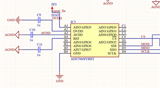
Part Number: ADS7066
Other Parts Discussed in Thread: OPA333

ads7066support.doc

  • Hello, 

    I am not sure if i understand your issue. 

    From what I can gather, the ADC is sampling the same channel, continuously, and each sample results in a different value, even though the input signal is DC. Is this understanding correct?

    Also, you have used the TEST_EN functionality on channel 6 to make sure you reading data correctly, and this has proven successful. you are correctly reading the expected 1.8V from channel 6.  If this is correct, then I do not suspect the driver code is the issue. 

    Can you share a schematic of the input signals?

    Regards

    Cynthia

  • Thank you for your reply!Cynthia
    I agree wholeheartedly with you that each sample results in a different value, even though the input signal is DC.During my debugging, this ADC only collected data of the internal fixed voltagefrom AIN6 。But according to the logic analyzer, the values of the fixed voltage collected in diagnostic mode vary by thousands of LSB. I don't think it's correct.
    For schematic,It's on the other computer. But I can share it with you tomorrow.regrettably.
    Look forward to your reply.
    Jeff
  • Jeff, 

    When using the Ch6 fixed voltage test, it is necessary to disconnect the input signal to Ch6, and leave it floating. If a signal is present at Ch6 input pin, then this can disrupt the fixed voltage test. 

    I looked through the code you provided, and there seems to be a lot of inconsistency, I cannot make out what the code is trying to do. I believe it has set 7 out of 8 channels to be digital outputs, only channel 1 is an analog input. 

    Would you do the following: connect the oscilloscope, or logic analyzer, to the digital bus, CS, SDI, SDO, SCLK

    Power cycle the supply to the ADS7066.

    Send the following commands, with CS held low: 0x08, 0x02, 0x80, grab  a screen shot of this transaction 

    Release CS to be high now. Then send three frames that consist of CS going from high to low, and low for 24 SCLK. During each frame, the SDI should be empty (0x00). and SDO should read 0xA5A5 for each frame. Please get a screen shot of this and share.

    Regards

    Cynthia

  • Cynthia,

    1,I have confirmed that CH6 is floating.

    2,The reason I set up only one analog input channel is to ensure that the channel is not disturbed by analog signals from other channels.  

    3 ,My code ensures that my SPI can successfully read and write registers

    4,If I need to read 0xA5A5 from SDO ,I must set FIX_PAT=1.But by doing so, I can't confirm whether the adc sample value is correct  or not.

    5,econfigure the ADC test FIX PAT

  • Thank you for sharing your schematic. 

    Since you are only using channel 5 as an analog input, you will need to configure the Pin Configuration register to: 0xDF, you currently have it to 0xBF

    Seeing how the fixed pattern works, this makes me believe that you can read data from the device correctly. It would have been better to include the frames where the SDI was being configured in the scope shot though. 

    To read data in manual mode, you need to set the Manual_Chid bits to channel 5 in the Channel_SEL register

    Address = 0x11, content= 0x05

    Once this is done, since you only want to sample that channel, you only need to provide new CS frames and Ch5 data will continue to be clocked out. Also confirm the input voltage at the ADC pin with a multimeter. 

    Please provide a scope shot of this configuration being complete. 

    Regards

    Cynthia

    • Configuration of all registers

    • The partial voltage of the lithium battery is  the DC signal input through  the follower...(1.59V)

    • test data 
    • I've tried everything, but I can't solve it.

  • Thank you for sharing your input schematic. 

    The opa333 is a great device, but not for driving ADC inputs at fast sampling rates. Note the OPA333 has a Gain Bandwidth of only 350Khz, this is not enough to drive the input signal correctly to the ADC for the ADC to result in an accurate measurement. This is likely why the ADS7066 is resulting in unexpected measurements. 

    With the OPA333, the fastest sampling rate the ADS7066 could be used at is 43.2 KSPS.  One quick way to confirm this is the source of the issue is to slow down the sampling rate by elongating the time CS is high to about 23us.

    With CS high for 23us between each frame, this will provide longer time for the OPA333 to drive the input signal to the ADC. Doing this you should see a significant improvement in ADC measurement  results.  In addition, the RC circuit is not optimized with the OPA333. I would also suggest changing the RC circuit at the ADC input, the resistor is too big, I suggest a value between 10K to 1K ohm and a capacitor between 300pF to 910pF. 

    If you wish to use the ADS7066 at full sampling rate of 250KSPS, you will need an op amp with a GBW of at least 7Mhz.

    If your system cannot support a sampling rate as slow by the OPA333, it will need to be replaced with a higher GBW op amp. I would suggest the OPA320 or OPA325

    Looking at the scope shot. You are continuously sending write operations to the device, this is not necessary. You only need to send this command once. Any CS frame after this intended to read  ADC measurement data, the SDI can be held low and the device will output only Ch5 output data. 


    Regards

    Cynthia

  • Thank you so much for your assistance!!!The problem is out of the way now.

    Regards

    Jeff