This thread has been locked.

If you have a related question, please click the "Ask a related question" button in the top right corner. The newly created question will be automatically linked to this question.

ADS1298: Noise with lead-off detection

Part Number: ADS1298

Hi everyone, We are experiencing some troubles with production project. In first PCB we have not troubles, now we change some distances in analog interface to meet IEC requirements.
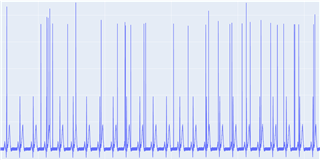
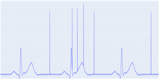
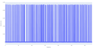
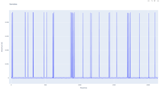
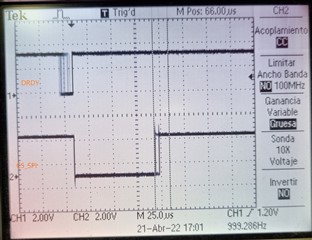
If we turn on the lead-off pull-up resistors (only pull-up) we have noise in this channel, but if we turn on the current source intead the pull-up resistor we have not noise in the correspondent channel.
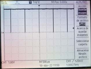
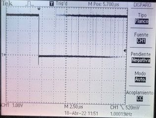
The noise is in a irregular time interval, but the amplitude it seems be the same every time. If we made a diff between consecutive points the difference in noise points is the same, then we think in a digital error. It looks like the correspondant voltage point is move in a fixed voltage.
We think the PCB is not the main problem, perhaps we are using a silicon with a know trouble?
Dou you have any information about similar problems?
Dou you experiment some like this?

While we are experimenting with the PCB, if we have some new we will tell you.

Regards

Martin

  • We were doing some experimentation.

    * Simulation
    We made a simulation to try to reproduce the problem. We think a noise in the AVDD voltage could be the cause of the noise, but our simulations results are we need a noise of 700mV in AVDD to made the same noise amplitude we measure. We put the scope in PCB AVDD and there is not noise, only are a floor noise smaller than 20mV peak to peak.

    * Series resistor input
    If we take off the the resistors in series to the signal path (surge protection and filtering) the problem disappears, there is not noise in signal.

    * External pull-up
    Instead the internal pull-up resistor we put an external 10M resistor in the ADS1298 input, with this circuital configuration we have the same problem, but a little different.
    With external 10M pull-up resistor we have the half amplitude peaks of noise, the ADS detects the lead-off (the comparator stills on) and the noise peaks tend to dissapears before some time.
    Then we test with 20M external pull-up resistor, and we have the half amplitud peak noise than we had with 10M external pull-up resistor.
     
    * Resume:
    Pull-up Noise amplitude
    Not pull-up Not noise
    10M internal ~5mV
    10M external ~2.5mV
    20M external ~1.25mV

    * Noise characteristics
    The noise is independent of if there is signal or not. The noise is like burst of peaks in a non repetitive way.
    Example of noise with 10M internal pull-up
    detal of noise with 10M internal pull-up
    Regars
    Martin
  • Hello Martin, 

    After we solve your other post, we'll take a look at this. Please give me 24 hours for the next update on this.

    Kind regards,
    Nick 

  • Hello Nick,

    Thanks for your response. Please, take note this is another project, this project is under production. The other post is about a project under development.

    I warn you so that you understand that some configurations could change between projects, for example in this project all the inputs are used.

    Thanks a lot,

    Kind regards,

    Martin

  • Hello Martin, 

    Duly noted, thank you for the clarification. We'll update you tomorrow.

    Kind regards,
    Nick

  • Hello Marvin, 

    Sorry for the delay. We need to ask a couple questions to help narrow down the issue: 

    1. Could you attempt this setup without using a simulator for your signal? Let's try to remove variables. 

    2. If you could recreate this noise on the ADS1298 EVM, that would also be a huge help for us since we can recreate it. 

    3. What does your DRDY signal look like during this?

    Kind regards,

    Nick

  • Hello Nick,

    1. We disconnect the patient simulator and shorted the inputs with a wire and the result is there are noise:
    We zoomed and the result was:

    2. We have not the evaluation module for ADS1298

    3. I attach the measured DRDY, in the first image you could see the DRDY is every 1ms as is expected:

    In the second image you could see the duration of DRDY is variable:


    Kind regards,
    Martin
  • Hello Martin,

    When the inputs are shorted, we should be seeing the signal stay low... Could you share what your board layout with the ADS1298 looks like? If you want to keep it off a public forum, we could open an email thread. 

    Looking at the DRDY signal, since the DRDY goes high on the falling edge of the SPI CLK, you could be seeing multiple DRDY/SPI_CLK interactions. Let's observe both DRDY and the SPI chip select, CS. See Figure 59. 


  • Hi Nick,

    I attached the scope captures of DRDY and CS_SPI. The first capture shows the DRDY frequency:


    The second capture shows the edge detail of both signals. The trigger was in the rising edge of DRDY:


    Kind regards,
    Martin
  • Hi Martin, 

    Those look about right. From here, could we get a copy of your configuration settings so we can try recreating this issue? 

    Kind regards,
    Nick 

  • Hi Nick, 

    This is the used configuration:

    void ADS_Init(void)
    {
        __delay_ms(1);
        CS_ADS = 1;
        PWDN_ADS = 1;
        Nop();
        RESET_ADS = 1;
        __delay_ms(200); // Minimun tPOR que es 2^18 * tclk
        // 2^18 * (1/2.048 MHz) = 0.128 seg
        RESET_ADS = 0;
        __delay_us(1); // 2*tclk = 0.97 us
        RESET_ADS = 1;
        __delay_us(10); // 18* tclk = 8.7 us
        ADS_Stop_Read_Data_Cont();
    //    ADS_write_register(ADS1298_CONFIG3_ADDR, VREFP_2 | PD_REFBUF_OFF | RLD_BUF_OFF);
        ADS_write_register(ADS1298_CONFIG3_ADDR, VREFP_2 | PD_REFBUF_ON | RLD_BUF_ON | RLDREF_INT);  //sensing and measuring of RLD
        __delay_ms(10); // no aclara cuanto esperar
        ADS_write_register(ADS1298_CONFIG1_ADDR, HR_ON | DAISY_OFF | CLK_OFF | DATA_RATE_MOD512); // High resolution, 1000SPS

        ADS_write_register(ADS1298_CONFIG2_ADDR, WCT_CHOP_VAR | INT_TEST_OFF | TEST_AMP1 | TEST_FREQ3);

        ADS_write_register(ADS1298_CH1SET_ADDR, PWR_UP | PGA_4 | CH_IN_NORMAL); //Normal mode
        ADS_write_register(ADS1298_CH2SET_ADDR, PWR_UP | PGA_4 | CH_IN_NORMAL);
        ADS_write_register(ADS1298_CH3SET_ADDR, PWR_UP | PGA_4 | CH_IN_NORMAL);
        ADS_write_register(ADS1298_CH4SET_ADDR, PWR_UP | PGA_4 | CH_IN_NORMAL);
        ADS_write_register(ADS1298_CH5SET_ADDR, PWR_UP | PGA_4 | CH_IN_NORMAL);
        ADS_write_register(ADS1298_CH6SET_ADDR, PWR_UP | PGA_4 | CH_IN_NORMAL);
        ADS_write_register(ADS1298_CH7SET_ADDR, PWR_UP | PGA_4 | CH_IN_NORMAL);

        ADS_write_register(ADS1298_CH8SET_ADDR, PWR_UP | PGA_4 | CH_IN_NORMAL);

        ADS_write_register(ADS1298_RLD_SENSP_ADDR, RLD1P_ON | RLD2P_OFF | RLD3P_OFF | RLD4P_OFF | RLD5P_OFF | RLD6P_OFF | RLD7P_OFF | RLD8P_OFF);
        ADS_write_register(ADS1298_RLD_SENSN_ADDR, RLD1N_ON | RLD2N_ON | RLD3N_OFF | RLD4N_OFF | RLD5N_OFF | RLD6N_OFF | RLD7N_OFF | RLD8N_OFF);


        ADS_write_register(ADS1298_WCT1_ADDR,WCTA_ON|WCTA_CH1_POS|aVF_CH6_OFF|aVL_CH5_OFF|aVR_CH7_OFF|aVR_CH4_OFF);
        ADS_write_register(ADS1298_WCT2_ADDR,WCTB_ON|WCTB_CH1_NEG|WCTC_ON|WCTC_CH2_NEG);

        ADS_write_register(ADS1298_LOFF_ADDR, LOFF_COMP_THRES_1|VLEAD_OFF_PUP | LEAD_OFF_FREQ_4);    // Detection with pull up resistors
        ADS_write_register(ADS1298_CONFIG4_ADDR, LOFF_COMP_ON | WCT_TO_RLD_OFF);

        ADS_write_register(ADS1298_LOFF_SENSP_ADDR, LOFF8P_ON | LOFF7P_ON | LOFF6P_ON | LOFF5P_ON | LOFF4P_ON | LOFF3P_ON | LOFF2P_OFF | LOFF1P_ON);
        ADS_write_register(ADS1298_LOFF_SENSN_ADDR, LOFF8N_OFF | LOFF7N_OFF | LOFF6N_OFF | LOFF5N_OFF | LOFF4N_OFF | LOFF3N_OFF | LOFF2N_ON| LOFF1N_ON);


        ADS_write_register(ADS1298_PACE_ADDR, PACE_CH2 | PACE_DETECT_BUFF_ON );

        ADS_Start_Conv(); // After this point DRDY should toggle a fclk/4096
        ADS_Read_Data_Cont();
    }
    Definition are the same as the other post.
    Kinds, regards
    Martin
  • FYI, just in case, I copy the definitions:

    /****************************RESP: Respiration Control Register***********************************************************/
        #define RESP 0x00                            /*[Default], no se usa en este chip*/
    /**************************************************************************************************************************/

    /********************************************Bits asociados a CONFIG4****************************************************************/

        /*Respiration modulation frequency */

        #define RESP_FREQ_64K 0x00                            /*64 KHz modulation clock*/
        #define RESP_FREQ_32K 0x20                            /*32 KHZ modulation clock*/
        #define RESP_FREQ_16K 0x40                            /*16 kHz square wave on GPIO3 and GPIO4*/
        #define RESP_FREQ_8K 0x60                            /*8 kHz square wave on GPIO3 and GPIO4*/
        #define RESP_FREQ_4K 0x80                            /*4 kHz square wave on GPIO3 and GPIO4*/
        #define RESP_FREQ_2K 0xA0                            /*2 kHz square wave on GPIO3 and GPIO4*/
        #define RESP_FREQ_1K 0xC0                            /*1 kHz square wave on GPIO3 and GPIO4*/
        #define RESP_FREQ_500 0xE0                            /*500 Hz square wave on GPIO3 and GPIO4*/


        /*Conversion mode*/

        #define SINGLE_SHOT             0x04
        #define CONT_MODE 0x00                            /*[Default]*/


        /*WCT to RLD Conection*/

        #define WCT_TO_RLD_ON           0x04
        #define WCT_TO_RLD_OFF 0x00                            /*[Default]*/


        /*Lead-Off comparator power down*/

        #define LOFF_COMP_ON            0x02
        #define LOFF_COMP_OFF 0x00                            /*[Default]*/

    /*********************************************************************************************************************/


    /***********************WCT1: Wilson Terminal and Augmented Lead Control Register **********************************/


        /* aVF_CH6: Enable (WCTA + WCTB)/2 to the negative input of channel 6*/

        #define aVF_CH6_ON              0x80         /*Enable */
        #define aVF_CH6_OFF             0x00         /*Disable [Default]*/


        /* aVL_CH5: Enable (WCTA + WCTC)/2 to the negative input of channel 5*/

        #define aVL_CH5_ON              0x40         /*Enable */
        #define aVL_CH5_OFF             0x00         /*Disable [Default]*/

        /* aVR_CH7: Enable (WCTB + WCTC)/2 to the negative input of channel 7*/

        #define aVR_CH7_ON              0x20         /*Enable */
        #define aVR_CH7_OFF             0x00         /*Disable [Default]*/

        /* aVR_CH4: Enable (WCTB + WCTC)/2 to the negative input of channel 4*/

        #define aVR_CH4_ON              0x10         /*Enable */
        #define aVR_CH4_OFF             0x00         /*Disable [Default]*/


        /* Power down WCTA*/

        #define WCTA_ON                 0x08         /*Powered On */
        #define WCTA_OFF                0x00         /*Powered Down [Default]*/

        /* WCT amplifier A channel selection ; typically connected to RA electrode*/


        #define WCTA_CH1_POS            0x00         /*CH1 positive input connected to WCTA amp [Default]*/
        #define WCTA_CH1_NEG            0x01         /*CH1 negative input connected to WCTA amp*/
        #define WCTA_CH2_POS            0x02         /*CH2 positive input connected to WCTA amp*/
        #define WCTA_CH2_NEG            0x03         /*CH2 negative input connected to WCTA amp*/
        #define WCTA_CH3_POS            0x04         /*CH3 positive input connected to WCTA amp*/
        #define WCTA_CH3_NEG            0x05         /*CH3 negative input connected to WCTA amp*/
        #define WCTA_CH4_POS            0x06         /*CH4 positive input connected to WCTA amp*/
        #define WCTA_CH5_NEG            0x07         /*CH5 negative input connected to WCTA amp*/

    /********************************************************************************************/

    /*****************WCT2: Wilson Terminal Control Register************************************/

        /*Power down WCTC*/

        #define WCTC_ON                 0x80         /*Powered On */
        #define WCTC_OFF                0x00         /*Powered Down [Default]*/

        /*Power Down WCTB*/

        #define WCTB_ON                 0x40         /*Powered On */
        #define WCTB_OFF                0x00         /*Powered Down [Default]*/

        /*WCT amplifier B selection; typically connected to LA electrode */

        #define WCTB_CH1_POS            0x00         /*CH1 positive input connected to WCTB amp [Default]*/
        #define WCTB_CH1_NEG            0x08         /*CH1 positive input connected to WCTB amp */
        #define WCTB_CH2_POS            0x10         /*CH2 positive input connected to WCTB amp */
        #define WCTB_CH2_NEG            0x18         /*CH2 positive input connected to WCTB amp */
        #define WCTB_CH3_POS            0x20         /*CH3 positive input connected to WCTB amp */
        #define WCTB_CH3_NEG            0x28         /*CH3 positive input connected to WCTB amp */
        #define WCTB_CH4_POS            0x30         /*CH4 positive input connected to WCTB amp */
        #define WCTB_CH4_NEG            0x38         /*CH5 positive input connected to WCTB amp */

        /*WCT amplifier C selection; typically connected to LL electrode */

        #define WCTC_CH1_POS            0x00         /*CH1 positive input connected to WCTC amp [Default]*/
        #define WCTC_CH1_NEG            0x01         /*CH1 positive input connected to WCTC amp */
        #define WCTC_CH2_POS            0x02         /*CH2 positive input connected to WCTC amp */
        #define WCTC_CH2_NEG            0x03         /*CH2 positive input connected to WCTC amp */
        #define WCTC_CH3_POS            0x04         /*CH3 positive input connected to WCTC amp */
        #define WCTC_CH3_NEG            0x05         /*CH3 positive input connected to WCTC amp */
        #define WCTC_CH4_POS            0x06         /*CH4 positive input connected to WCTC amp */
        #define WCTC_CH4_NEG            0x07         /*CH4 positive input connected to WCTC amp */

    /*********************************************************************************************/


    /******************************** Opcodes Commands Definitions ********************************/

    /* System Commands */

    #define ADS_WAKEUP              0x02        /*Wake up from stand by mode*/
                                                /*cualquier comando subsiguiente tiene que ir despues de 4tclk */
    #define ADS_STANDBY             0x04        /*Enter stand by mode*/
    #define ADS_RESET_CMD           0x06        /*Reset the device*/
                                                /*se necesitan 18 tclk para el reset. no enviar comandos mientras tanto*/
    #define ADS_START               0x08        /*Start/restart (synchronize) conversions*/
    #define ADS_STOP                0x0A        /*Stop conversion*/

    /* Data Read Commands */

    #define ADS_RDATAC              0x10        /*Enable Read data continuous mode*/
                                                /*This mode is the dafault mode at power up*/
    #define ADS_SDATAC              0x11        /*Stop read data continuously mode*/
    #define ADS_RDATA               0x12        /*Read data by command; supports multiple readback*/

    /* Register Read Commands */

    #define RREG
    #define WREG


    /******************** Address Registers ********************************************/

    /* Global Settings Across Channels*/


    #define ADS1298_CONFIG1_ADDR                0x01
    #define ADS1298_CONFIG2_ADDR                0x02
    #define ADS1298_CONFIG3_ADDR                0x03
    #define ADS1298_LOFF_ADDR                   0x04


    /* Channel Specific Settings*/

    #define ADS1298_CH1SET_ADDR                 0x05
    #define ADS1298_CH2SET_ADDR                 0x06
    #define ADS1298_CH3SET_ADDR                 0x07
    #define ADS1298_CH4SET_ADDR                 0x08
    #define ADS1298_CH5SET_ADDR                 0x09
    #define ADS1298_CH6SET_ADDR                 0x0A
    #define ADS1298_CH7SET_ADDR                 0x0B
    #define ADS1298_CH8SET_ADDR                 0x0C
    #define ADS1298_RLD_SENSP_ADDR              0x0D
    #define ADS1298_RLD_SENSN_ADDR              0x0E
    #define ADS1298_LOFF_SENSP_ADDR             0x0F
    #define ADS1298_LOFF_SENSN_ADDR             0x10
    #define ADS1298_FLIP_ADDR                   0x11

    /*Lead-Off Status Register (Read Only Registers)*/

    #define ADS1298_LOFF_STATP_ADDR             0x12
    #define ADS1298_LOFF_STATN_ADRR             0x13

    /*GPIO and Other Registers*/

    #define ADS1298_GPIO_ADDR                   0x14
    #define ADS1298_PACE_ADDR                   0x15
    #define ADS1298_RESP_ADDR                   0x16
    #define ADS1298_CONFIG4_ADDR                0x17
    #define ADS1298_WCT1_ADDR                   0x18
    #define ADS1298_WCT2_ADDR                   0x19

    Kind regards

    Martin

  • Hi Martin, 

    Thanks for the detail, it'll take me a day or two to audit, but I'll have it done by the time we have our support call. 

    Let's host a call so we can better dedicate support versus these two threads. I'm going to reach out via email. 

    Kind regards,
    Nick Z

  • Hi Martin, 

    Since this conversation was taken to email and a meeting to solve the problem, I'll be closing the thread.

    Please use our email-thread for any follow ups on this topic, or open a new post for further support. 

    Kind regards,
    Nick Z