This thread has been locked.

If you have a related question, please click the "Ask a related question" button in the top right corner. The newly created question will be automatically linked to this question.

TI-JESD204-IP: SYSREF and timing question for ref design connecting to xilinx VC707 and DAC39j84

Part Number: TI-JESD204-IP
Other Parts Discussed in Thread: DAC39J84

Hi, I downloaded TI-JESD204B IP and use zc706_8b10b ref design for VC707 fpga board and DAC39j84. I use LMFS=8411 and HD=1. Here are few questions that bug me during my implementation:

1. the ref design does not have sysref input, so do we need sysref input if we only connect one DAC39j84 board? Does it mean if we don't use multi DAC board, we don't need sysref signal? Or we need to add sysref in real design?

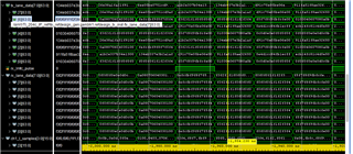
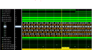
2. My design is not working, and when I checked the ILA, I found that tx_lane_start_of_frame is 1 but tx_lane_start_of_multiframe is 0. Does that mean there's something wrong in my design? I'm kind of confused about this part.

3. We won't have  ILAS process for tx if cfg_tx_ilas_test_mode=0 right? If it's 1, whst is the ILAS series?  Is it 4 byte from K28.0 to K28.3?

4. I suffered timing failure meanly between clkout0 and sys_clk_sys_pll1 during setup period, will this be a problem for the design?

Thanks advance for your help.

Best,

Shuyi

  • Hi,

    I have listed answers to your points below:

    1. SYSREF is needed if you need to implement deterministic latency, or if you need to synchronize multiple DACs and FPGA IPs. If this is not necessary, SYSREF can be tied to ‘0’
    2. Yes. You should see the multiframe signal toggle as well. I am not sure what can cause this, though. 
    3. The ILAS test mode input is an internal test mode only and should be tied to ‘0’
    4. the path between the freerun clock and other clocks is a  false path. If you are seeing violations there, you can ignore the same

    Regards,

    Ameet

  • Thank you so much for your answer. I'm still a little bit confused when do we need to implement deterministic latency? I read some file about it but still a little bit confused.

    Plus, here's another question I faced in simulation, I connected adc_lane_rx directly to dac_lane_tx to see if the loop is right. But I found that the rx_lane_data I received is different from tx_lane_data I sent. For all the 8 rx_lane_data it all repeat the same data from tx_lane 6 like this:

    I'm so confused and I checked for both rx and tx LMFS=8411 and HD=1, and tx_lane 0 &1 transmit sinei, tx_lane 2&3 transmit sineq, lane 4 &5 are the same as 0 &1, lane 6 & 7 are the same as 2 & 3. I checked dac_lane_tx and found that all 8 lane transmit the same data after K28.5:

    What cause this happen for the correct tx_lane_data but partically correct dac_lane_tx? Why 8 lane of dac_lane_tx repeat only one lane of tx_lane_data? I thought each lane of output should transmit the corresponding lane of input. And do you have any official simulation file for the ip?

    Thanks advance for your help.

  • Hi,

    Deterministic latency will be dependent on your application needs. The end to end delay from the front end of the data converter to lane data of the JESD IP in the FPGA is constant when the link is working, but this delay can change by up to 10-15ns across link power cycles. If this delay is not an issue, then you don’t need deterministic latency 

    The other issue you are seeing is probably a Vivado simulation problem. Please check the jesd link params vh file and update the *LANE_MAP parameters to {3’d7, 3’d6, 3’d5….etc}

    The simulator is overriding all lane map values to 0, so all Rx lanes are showing data received on lane 0. This problem is not seen with synthesis or other simulators like Cadence or Mentor. 

    Regards,

    Ameet