A related question is a question created from another question. When the related question is created, it will be automatically linked to the original question.
If you have a related question, please click the "Ask a related question" button in the top right corner. The newly created question will be automatically linked to this question.
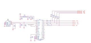
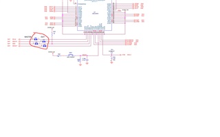
ADC3444EVM: The SPI pin of the adc344evm board is linked to USB control by default, so if we want to realize SPI control through FPGA with the fmc-adc-adapter board, we now need to solder R71, R72, R73, r74 off, and R68, R69, r70, R71 on?
You are correct in the required modifications. The ADC3444 can accept SPI levels of up to 3.3V despite having a digital supply rail of 1.8V. This is to accommodate a larger variety of SPI drivers which may be using 3.3V logic. If you ensure that your FPGA level is 3.3V or lower then there should be no further actions.
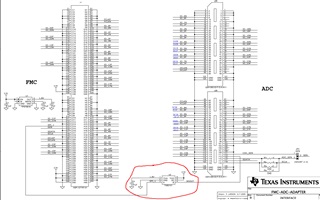
Thank you very much for your answer. The fmc-adc-adapter card converts the SDUOT signal from 3.3V to 1.8V, and the FPGA control signal is 1.8V. In addition, I have a little suggestion and doubt. I want to consider why it is not possible to switch the SPI signal path by jumper, but by 0 ohm resistors? Isn't JP2, JP3, JP4,JP5 on the adc344evm board redundant? Is there any other way without SPI control? There are some misunderstandings here.
These jumpers come in handy for a few reasons. Mainly, these are used for probing the SPI lines on the EVM with an oscilloscope, however these jumpers also allow for the SPI line to be broken from the FTDI circuitry so you can connect your own SPI wires from any other external source, such as a microcontroller. On our newer EVM designs, we are using MUX switches and a single jumper to switch from SPI using the FTDI part to using SPI over the FPGA FMC connector.