This thread has been locked.

If you have a related question, please click the "Ask a related question" button in the top right corner. The newly created question will be automatically linked to this question.

ADS131M04EVM: DOUT not working and DRDY line consistently outputting never going down to 0V

Part Number: ADS131M04EVM

I am trying to use my evaluation boards together for the PIC and the ADS, so that I can show communication and reading of ADC channel readings. As for the configuration between the two...

1. I have the PIC eval board wired to the EVM for signals, SCLK, DIN, DOUT, CS, DRDY, SYNC/RST. I have wires on J6 going between the boards.

2. I do not have the PHI board connected.

3. Using a 3.3V external supply applied to test points AVDD and DVDD on the EVM. 

4. The jumper is removed on JP9 for the LDO/MSP selection.

5. I did not remove R45. 

On the scope I verified the signals when writing (CS, SCLK @ 1MHz, DIN) lines are correctly outputting to the ADS. When I look at DOUT, the output is not clean. Only seeing noise where the SCLK and DIN is present. Never reaching 3.3V and having a proper pulse width. The pulses expecting the returned data are not there; just seems like noise spikes (very thin and never reaching 3.3V).

DRDY never reaches 0V, it hovers around half a volt most of the time with blimps at around 4kHz. This is seen no matter if the channels are enabled or disabled. I thought DRDY is to be high. On the PIC I make sure it is latched high. What could be causing this behavior?

I read the EVM data sheet and the ADS one too. My goal is to be able to read and return readings from each ADS channel. 

My PIC is setup for SPI1 Mode. 1MHz serial clock. 

How can I verify that the ADC is getting the written data, if the DOUT is not outputting right?

Additional info, when I received the EVM, I used the PHI with GUI. I was able to capture and read/write registers. On the scope, the signals for DIN/DOUT were very noisy pulses. 

  • Hello Tricia,

    Thanks for posting on the forum! I agree with your set up for the SPI bus and power supplies.

    You are partially correct though, nDRDY is supposed to start toggling as soon as Power On Reset (POR) is satisfied (i.e. the AVDD and DVDD rails are up). It won't remain high but it will mostly stay low and then toggle high when new data is ready. Before we start using SPI commands, we need to make sure the device started up correctly.

    I have two theories about this. First, what is SYNC/RESET? From the PIC side it will be should be configured as an output and held high; if its held low the device will continually stay in reset and try to wakeup after many CLKIN cycles. The second theory might be related to your statement: 

    I thought DRDY is to be high. On the PIC I make sure it is latched high

    I'm confused what you mean by latched high. The pin on the PIC should be configured as an input so I'm not sure what "latched high" means. A nonzero voltage on nDRDY would imply that there might be bus contention. If nDRDY is an output on ADC side that's trying to drive low for the most part and the PIC is trying to hold it high then the voltage might be somewhere in-between.

    Those are some of the basic possibilities. After that, we need to start probing AVDD and DVDD at the ADC pins to make sure they've powered up correctly.

    Best,

    -Cole

  • Cole,

    So nDRDY pulsing is a good thing. So it looks like POR is satisfied. At the PIC this is an input. I have it as such. I removed setting the pin high on powerup.

    The SYNC/RESET is an output of the PIC and is placed high on power up and remains high.

    I have probed the ADC AVDD and DVDD pins on both sides of each resistor, R36 and R37, on the EVM and read 3.3V.

    As for DOUT (output of ADC/Input to PIC), this is set at a level of around 500mV. I probed this on the scope with the SCLK and notice spikes at every rising edge of the clock. They are barely 20ns width spikes. Is this a ground issue? 

  • Hello Tricia,

    In general, yes, nDRDY pulsing just after power up should be a good thing. To clarify, nDRDY will be mostly low but pulse high at the rate of the default data rate (I think 4kHz is the default if you have ~8MHz clock for CLKIN). If the pulsing matches that behavior then you should be good.

    Hmm, 20ns pulse widths would as wide as a 25MHz SCLK which is the max frequency accepted by the device. I assume you're running much slower. There might be something there but its not obvious. The level of overshoot might be helpful too if you can measure that. Sometimes very high overshoot can link to a GNDing problem. Sometimes, its just the inductance of jumping wires between boards.

    500mV barely meets the VIL and VOL specs but its clearly much too high for a typical system. But you've probed a "low" state for some for nDRDY, it is also 500mV for a low? Or is it just DOUT? If its just DOUT, there might be a settings issue you need to consider in the processor. You might have it as an input but there might be some other contention on the line. Kind of what I explained before. If it is both then "low" states are sitting at 500mV then, yes, it might be a grounding issue and I don't have a good recommendation besides shortening wires or jumping more wires between the EVM and the PIC board.

    If you have scope screenshots feel free to send them my way. If we don't get anywhere with this avenue, I might need you to grab a logical analyzer and double check what you're sending is what you intend.

    Best,

    -Cole

  • Good day,

    I now see a good DOUT pulse width. I am struggling on reading back all four channels readings. I send the NULL command but it seems the SCLK is only shown when I write a byte but not when reading a byte. Maybe it is the routine in the PIC that does not provide a clock signal. I am using a Microchip 8 bit PIC for the main processor.

  • I found a routine that will send multiple bytes (0's) reading after each byte sent to the ADC and notice DOUT to be outputting. But each byte value is one bit logic shift from the previous byte received. So for example, I am seeing 0x040810 , 0x204080, 0x020408. I am keeping the default width of 24 bit. I do not have any potential (v) on any of the ADC input channels.

  • I read about the SYNC line to pull it down to resynchronize the ADC conversions and reset FIFOs. By doing that the values are more expected and less sporadic.

    As for the EVM, when using an external input voltage value in a single-ended input, I placed the jumper on pins5 & 6 for all. I tried to apply a 1.5V value on pin 1 of J1 (terminal block) and the results did not change. I would expect the counts to be higher than what I was previous seeing.

  • Hi Tricia,

    Yes, I was going to recommend clearing the FIFO for consistent data. Reading twice, throwing the results out, and reading a third time is a bit easier if you don't want to deal with SYNC timing. I'd also encourage you to read the contents of the STATUS register as part of the NULL command. You only gave me 3 channels of data in the last post and I was expecting to see all 4 channels which would have resulted in an error and inconsistent data if they were not all clocked out.

    Not having voltage on the inputs is the equivalent of floating and usually results in codes associated with GND'ing the inputs to show the offset voltage. Floating is inherently unpredictable and I recommend GND'ing the inputs and translating code to voltage and comparing that number to the offset voltage spec. If it falls within the range, then you probably have the correct value.


    You applied 1.5V to pin1 of J1 which would be AIN0P and AIN0N is GND or 0V. And I assume you connected the negative part of the 1.5V supply to GND. Usually this would change the input pretty obviously. I would encourage you to translate the code to the voltage and see what the ADC is actually reading. Then, I'd recommend ensuring the FIFO is not full when you're collecting this data. 

    Best,

    -Cole

  • I have jumpers on the JPs for each channel on pins 5 & 6 which would ground the negative side (looking at the schematic of the EVM). I also placed jumpers on pins 1 & 2 also to ground the positive side, in order to see how consistent the return values (counts) were. (I gather all bytes 15 total, first three status, remaining ch1 to ch4). Sorry I do not have the status response to report.

    Ch1 range 940 to 1017

    Ch2 range 875 to 930

    Ch3 range 1386 to 1447

    Ch4 range 648 to 743

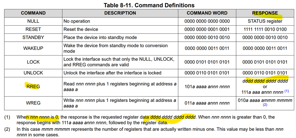
    When reading a single register, I do not have to read multiple byte sets (24 bit default width), only 3 bytes correct? 

    From what I read the only way to clear the FIFO is with pulling the SYNC signal down for a short time. Am I wrong? 

    The NULL command will return STATUS for its response in the first byte set. But will still need to read all channels data to make sure the ADC is not out of sync. Is this a correct statement?

  • Hello Tricia,

    Yes, that's how I would set up the input offset test as well. Ch3 looks a bit high but something tells me this would fall down within spec with some averaging to get rid of the noise. So, the device looks like it is operating correctly.

    I was expecting you to do the last step of calculating the code to voltage and look at the spec. If you don't know how to do that, here's a blog: https://e2e.ti.com/blogs_/archives/b/precisionhub/posts/it-s-in-the-math-how-to-convert-adc-code-to-a-voltage-part-1 

    When reading a single register, I do not have to read multiple byte sets (24 bit default width), only 3 bytes correct? 

    You got it, those first 16 bits in the response will be the data, there will be no more actual data. That being said, 24 bits is still a constant word size determined by WLENGTH. You'll still need to clock out a 24 bit long word even though most of those last bits will be zero. Hope that answers it.

    From what I read the only way to clear the FIFO is with pulling the SYNC signal down for a short time. Am I wrong? 

    You're correct. Reading two packets of data is equivalent as well. There's some more text about how to do that in the datasheet.

    The NULL command will return STATUS for its response in the first byte set. But will still need to read all channels data to make sure the ADC is not out of sync. Is this a correct statement?

    That's correct. The only exception is if you want to skip CRC. There's a short SPI frame section in the datasheet with more info.

    Other comments:

    It's clear that you're a newer engineer. If you have not already, I highly recommend reviewing the compiled FAQ: https://e2e.ti.com/support/data-converters-group/data-converters/f/data-converters-forum/1060610/faq-have-a-question-about-adcs-click-here-for-faqs-resources-and-more 

    And if you have not seen our training series on ADCs, I highly suggest you check out our video series: [Video Series] TI Precision Labs – ADCs

    I do want to reassure you that your questions have mostly been very specific questions about the device, which is perfect. If you have not checked out some of these resources, it will accelerate your learning.

    Best,

    -Cole

  • Cole,

    Thank you for confirming. One additional question about the EVM, I have currently jumpers to ground both pos and neg inputs for each channel. I would like to provide a voltage and have tried to apply a constant voltage on one channel but I do not see the counts jump. Is there a special configuration for the channel on the EVM. When I applied the voltage I removed the jumper to the positive side.

    Otherwise I have been getting consistent responses from the ADC EVM to my PIC.

  • Hi Tricia, 

    You're setting up the HW correctly by removing the jumper from the positive input. From the ADC settings side, if you see a nonzero code then the ADC channels are enabled, which is really the only setting that can change the results this rapidly. The only external setting is SYNC/RESET but you can speak to the device using SPI so there shouldn't be any issues there. Have you confirmed that you could write to a register so that it doesn't match the default, read it back, and confirm the device accepted the write?

    I'd like to take a different route. You've mentioned that this is the EVM. Do you have the GUI and other external controller board (PHI board) that would provided with the EVM kit? I'd like to see you collect some data using the GUI and send a screenshot of the main screen. If you can get the GUI running, we can get a known good set up vs. your set up and we can easily rule out the HW configuration for the EVM to be the issue.

    Thanks,

    -Cole