This thread has been locked.

If you have a related question, please click the "Ask a related question" button in the top right corner. The newly created question will be automatically linked to this question.

ADS54J69EVM: Configuration file is missing

Part Number: ADS54J69EVM
Other Parts Discussed in Thread: ADS54J60EVM, ADS54J60, ADS54J69, LMK04828, TSW14J57EVM

Hello TI experts,

My customer tests ADS54J69EVM now, and here is one problem.

They tried to evaluate 2.3.1.7 in the User's Guide, but they could not find “ADS654J69_2X_dec_lowpass_4222.cfg” in any folder.

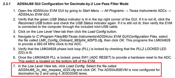
Could you check where this configuration file is? or please attach this file with your post.

Best regards,

Chase

  • Hi Chase,

    I did not have an ADS54J69EVM on hand in the lab, so I tested this with a ADS54J60EVM. I was able to capture a noise floor following the procedure 'ADS54J69 GUI Configuration for Decimate-by-2 Low Pass Filter Mode', and loading the 'ADS54J60_2x_dec_lowpass_4222.cfg' file and selecting 'ADS54J69_2x_4222' in HSDC Pro. 

    Please try this and let us know if you run into issues.

    Regards, Amy

  • Dear Amy,

    Thank you for your support.

    My customer did some tests so far, but they could not confirmed 250MHz clock from LMK04828. I think it would be 250MHz.

    (they confirmed 122.88MHz clock to LMK04828.)

    Please check this issue. Thanks.

    Best regards,

    Chase

  • Chase,

    Can you ask the customer to provide us with the LMK04828 clocking tabs from the GUI? Is the customer expecting a 250MHz output from the LMK04828 to clock the ADC? The config file which Amy posted should also work for the ADS54J69 without any issue, just may need to modify the clocking. Posting the 4 LMK04828 tabs (PLL1 configuration, PLL2 configuration, SYSREF and SYNC, Clock Outputs) will help us debug this much faster.

    Regards, Chase

  • Dear Chase W,

    Thank you for your support. I attach a screenshot of LMK04828 tab of GUI program.

    and here is 1 more questions ;

    - Should I enter some commands after loading configuration file for test? or just load configuration file and all setting is done for test?

    Best regards,

    Chase

  • Chase,

    The missing configuration file is attached.

    Regards,

    Jim

    8203.ADS54J69_2x_dec_lowpass_4222.cfg

  • *** Dear jim s,

    Thank you for your support.

    My customer tested configuration file you noticed, but the result was same. Could you check it again please?

    *** Dear Chase W, Amy,

    Please take a look of screenshot and notice me if there are anything to change.

    and here are more questions ;

    1. Should I enter some commands after loading configuration file for test? or just load configuration file and all setting is done for test?

    2. How can we check the clock signal on U4 (P1 and P2 -> FPGA_JESD_CLKP/M & P62 and P63 -> CLK_LAO_0P/M) using oscilloscope?

    Do we need connecting any resistor between these 2 pins (P/M) or just contact GND of probe to any pins?

    Best regards,

    Chase

  • Chase,

    After completing step 7 in section 2.3.1, is LED D2 illuminated on the ADC EVM? If this LED is "ON", after clicking on "Capture" on HSDC Pro GUI, what is the status of the 8 status LED's on the TSW14J56EVM or TSW14J57EVM that you are connecting the ADC EVM to? 

    Send a screen shot of HSDC Pro GUI after clicking on the "Send" button.  

    Regards,

    Jim 

  • Dear jim s,

    Thank you for your support.

    my customer does not use TSW14J56EVM or TSW14J57EVM, instead they want to make capture board using FPGA and their own technology.

    so we want to know check that ADS54J69EVM working properly without capture board.

    1. How can we know that this EVM working? how about check the clock frequency from LMK04828?

    most of all we are worried about 250MHz clock frequency from LMK04828. How can we check this clock?

    2. we want to know starting test in EVM GUI. there any start button or other icons.

    please check these 2 issues. Thanks.

    Best regards,

    Chase

  • Chase,

    There are no built-in self-test functions available for our ADC EVM. The best we could do is offer a configuration file containing register sequence which we know works for the ADC on our setup. The problem with this is that the customer will be responsible for the debug on their custom capture card.

    Thanks, Chase

  • Checking the clock frequency will only tell you that the LMK04828 output dividers are setup correctly, which can be done very easily by simply looking at the GUI Clock Outputs page.

  • Dear Chase W,

    Thank you for your support.

    Where should I look in the GUI if the LMK04828 output cannot be observed?

    Best regards,

    Chase

  • Chase.

    After loading the LMK config file mentioned in the User's Guide, make sure LED D2 (PLL2_LOCKED) turns on. If this does not turn on, there is something wrong with your setup.

    With D2 "ON", go to the LMK0428 Clock Outputs tab in the GUI that is shown below and set the DCLK Divider for both CLKout 0 and 1 and CLKout 12 and 13 to "32". Uncheck "Group Powerdown" for CLKout 12 and 13 as the config file powers down this output by default.

    Your settings should like as shown below. You should now see a 92.16MHz clock on capacitors C93, C97, C79 and C80 which are located on the bottom of the EVM near the LMK04828 (U4). This frequency is the VCO frequency from PLL2 (2949.12MHz) divided by 32. 

    Regards,

    Jim

  • Dear jim s / Chase W,

    Thank you for your support.

    My customer did some tests for clock output of LMK04828, but they could not see the clock what they want.

    please see the screenshot of settings below ;

    They just checked 92.18MHz clock signal with the settings.

    As I said they will use Xilinx FPGA (Ultrascale+ AUP25), so they need the clock which is compatible with JESD204B IP. (100MHz, 125MHz, 156.25MHz, 250MHz and so on)

    I think there are some reference settings for JESD204B IP. could you check the initial setting for it? (especially PLL1, PLL2 and Clock output tab)

    Best regards,

    Chase

  • Chase,

    With the current VCXO that is populated on the EVM (122.88MHz), they will only be able to generate clock frequencies that are are a multiple of this frequency (122.88MHz, 245.76MHz, 368.64MHz, ect...). For the frequencies they need, they will have to either provide an external clock to the board or change the VCXO device. If they change this part to a 100MHz VCXO, they will be able to create 100MHz, 125MHz, 156.25, 250MHz and so on.

    If they provide an external 2500MHz clock to SMA J6, they can generate these frequencies using the LMK04828 in clock distribution mode.

    Let me know which option the customer prefers to use and I will send the LMK settings for this approach.

    Regards,

    Jim

  • Dear jim s,

    Thank you for your support.

    They prefer changing internal VCXO from 122.88MHz to 100 MHz.

    Could you check the setting for it? and if there should be changed to other settings (PLL1, PLL2, etc..)

    Best regards,

    Chase

  • Chase,

    With the VCXO at 100MHz, the attached LMK config file will create a 1GHz clock for the ADC and 100MHz for the two clocks going to the FPGA.

    Regards,

    Jim

    LMK_Config_Onboard_1000_MSPS_FPGA_100M.cfg

  • Dear jim s,

    My customer is still testing with 100MHz VCXO and configuration file which you gave to me.

    I will share the result when the test is done.

    Best regards,

    Chase