This thread has been locked.
If you have a related question, please click the "Ask a related question" button in the top right corner. The newly created question will be automatically linked to this question.
Hi,
I'm struggling with the SPI communication.
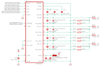
Schematic:
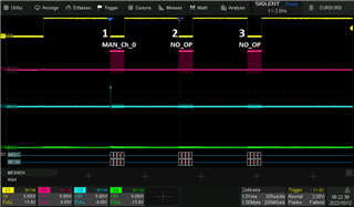
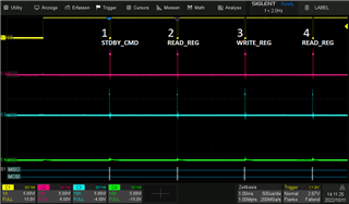
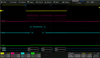
Complete Sequence (implemented test sequence):
(similar issue: ADS8664: ADS8664 spi communication - Data converters forum - Data converters - TI E2E support forums)
Sequence 1 - standby command:
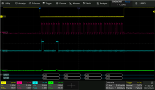
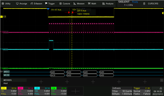
Sequence 2 - read register 0x17:
Expected: 0xF0
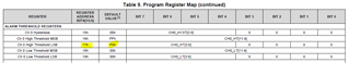
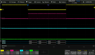
Sequence 3 - write register 0x17:
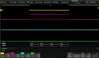
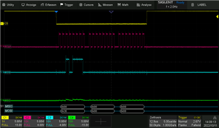
Sequence 4 - read register 0x17:
Expected: 0xA0
MISO is still 0x00, what could be the reason?
Thanks a lot.
Regards,
Sergei
Hi Sergei,
Thank you for your post. Can you disable standby command to check for test purpose? Are you able to get correct conversion data without programming any registers (default mode)? It seems like your MISO (SDO) is shorted to GND or forced to low, please check your hardware as well.
Regards,
Dale
Hi Dale,
1) Can you disable standby command to check for test purpose?
-> same behavior
2) Are you able to get correct conversion data without programming any registers (default mode)?
-> no, AIN_0P measured value = ~1V (multimeter), expected: data unequal 0x00
Complete Sequence (for test purpose with reduced SCLK=156kHz):
Sequence 1 - MAN_Ch_0:
Sequence 2 - NO_OP:
Sequence 3 - NO_OP:
3) please check your hardware as well
-> I checked CS,SCLK,MOSI,MISO, should be fine (no short, correct wiring)
Questions:
- Is the SPI mode correct? Timing dependencies/requirements?
- Power up dependencies? DVDD vs. AVDD vs. AIN_xP?
- How can I check, that the ADS8664 works in a proper way? Is it possible to damage the chip? (we observe the erroneous behavior an all boards)
Thanks a lot for your help.
Regards,
Sergei
Hi Sergei,
Your commands to the ADC are correct. I just found one issue in your schematic and hardware:
These should be the reasons you ADC is not working. PS: when ADS8664's input is floating, you will see an approximate 2.25V on the AINP and the corresponding conversion code on the SDO output for +/-2.5V default range because this is an internal bias voltage on the ADC. When an analog signal is applied to the ADC's input, you will not able to see this bias voltage and you will get conversion code for your analog input signal.
Normally you can check and measure the voltage on the REFIO and REFCAP pin, you should see approximate 4.096V since your are shorting the /REFSEL pin to GND and selecting internal voltage reference. Also, you can check the conversion code to see if it matches your analog input signal, DC input is a simple signal to check. These are basic steps to check if ADC is working.
Regards,
Dale
The thread was closed- by the poster, hardware connection (AGND and ADVDD pins were not connected) should be the root reason to cause the issue. This is just a note for other people's benefits in the future,