This thread has been locked.

If you have a related question, please click the "Ask a related question" button in the top right corner. The newly created question will be automatically linked to this question.

DAC7578: DAC7578 resistor Calculation

Part Number: DAC7578
Other Parts Discussed in Thread: DAC53204, TPS7A57

Hi,

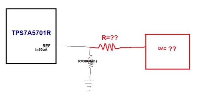
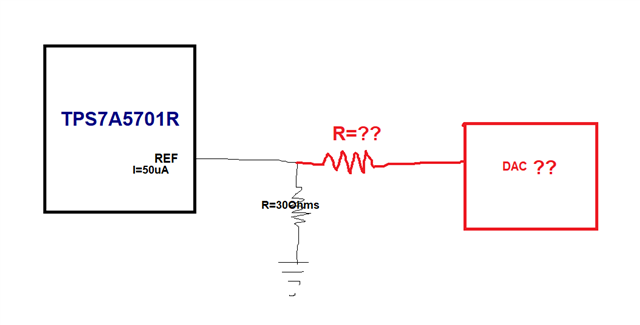
We are using DAC7578 for voltage margining. We are going to voltage margin with the help of resistor. We are forcing the voltage through the resistor for margining. Kindly help us in calculating the series resistor and can anyone pls tell how to calculate it.

Thanks

S Sathya shree 

  • Hi Sathya, take a look a this training:

    https://training.ti.com/voltage-regulator-margining-precision-dacs

    Also, the DAC53204 would be a great choice for this as well.

    Thanks,

    Paul

  • I would like to add one more thing, we are using TPS7A5701RTER LDO in our design. In this LDO we have only one resistor Rref to get the required output voltage. With this can we do voltage margining?. Is this fine to use this LDO. If it is fine means what about the series resistor of DAC. Can you please clarify how to find the full scale voltage of any DAC and VDACN.

  • We need 8 channel DAC. Kindly suggest us 8 channel DAC. Our LDO part number is TPS7A5701RTER.

    As TPS7A5701R has one reference resistor for setting output voltage, need guidance in calculating series resistor. Kindly help us in calculating it.

  • Hi Sathya,

    Consider using a current output DAC rather than a voltage output DAC.  Our DAC53204 (4 channels) has a current output range that be used in parallel with the 50uA reference current from the LDO.  The DAC can contribute additional current to increase the output voltage, or sink current to decrease the output voltage.  This would not require any additional resistor.  In addition, the DAC53204 can support true high-z operation at startup, so you do not need to worry about that condition.

    See this document:

    Voltage margining and scaling circuit with current output smart DAC

    Thanks,

    Paul

  • Hi Paul,

    With 50uA LDO and we need to margin 10% of output voltage using DAC. DAC need to sink or source 5uA as per our requirement.

    Do we need to consider any layout guidelines for implementing this.

  • Hi Sathya,

    There is not much of a layout concerns for this.  As a current source, we are less concerned about series resistance or parasitic capacitance. 

    Thanks,

    Paul

  • Hi Paul,

    Can you please guide in calculating the output in DAC53204, as we have seen many documents in that they have used two resistors for margining.

    Since we are going to use as current DAC with single resistor from LDO TPS7A57. Can you pls guide us how to do margining. We are going to margin 10% of 1.8V. Kindly guide us in implementing this.

  • Hi Paul,

    Gentle reminder for DAC53204 query.

    For DAC53204 reference calculation the below attached circuit diagram is given as the reference with two feedback resistors but in our SMPS design (TPS7A57) we have only one resistor.

    Please find the attached below snip of TI reference design calculation for DAC53204, according to TI calculation top resistor R1 is used in the calculation. But in our SMPS (TPS7A57) we have only one resistor (which is bottom resistor connected to gnd) for setting the output voltage and also Vref & Vnominal values are same.

    Kindly guide us in calculating I(margin) value.

    Below attached image is our SMPS design and we are going to do the voltage margining like this.

    Kindly resolve the issue as soon as possible.

  • Hi Sathya,

    It looks like the TPS7A57 actually discusses this in the datasheet using both the current output and voltage output modes of the DACx3204:

    The app note you are referring to talks about the two resistor (or three if a series resistor is required) method with the power supply having a voltage reference (typically called the FB or feedback pin). It looks like the TPS7A57 uses an internal current reference (50uA) to set the output voltage using a single Rref resistor. The smart DAC in current mode directly adds or subtracts from the internal current reference to adjust the output voltage. So the equation would be VOUT= Rref*(Iref ± Idac). 

    Please review sections 8.1.16 Current Mode Margining and 8.1.17 Voltage Mode Margining of the TPS7A57 datasheet. This will be more helpful to you than the other app note. Please let me know if you have any questions after that. 

    Best,

    Katlynne Jones

  • Hi Jones,

    Thank you for providing the input for DAC53204 using current mode for voltage margining.

    I need one more clarification for this DAC53204. We would like to know about voltage margining in voltage mode.

    Can you please guide us with the same spec as you mentioned above.

    LDO part number: TPS7A57

    Regards,

    S Sathya shree.

  • Hi Sathya,

    The TPS7A57 datasheet also has a section describing this: 

    The equation would similarly be: VOUT= Rref*(Iref + [(Vdac-Vnom)/Rdac]). Where Idac from the current output equation = [(Vdac-Vnom)/Rdac].

    Best,

    Katlynne Jones

  • Hi Jones,

    In the above snip, does Iout represent the margining current? For example, if we are going to margin +/-10% voltage of 1.8V, it will be 1.62V and 1.98V. According to this DAC, we are going to margin with current. Reference current for the LDO TPS7A57 is 50uA. if we give 5uA as margining, we will be getting 1.62V and 1.98V in the output. Does 5uA represents Iout and also Iout is same as Idac? Please clarify it. Guide us writing the register values.

    Thanks

    S Sathya shree

  • Hi Sathya,

    Yes, IOUT in equation 4 from the snip you share represents the current output from the DAC, which is the margining current in your case. 

    If your margining current is ±5μA then you should choose the smallest possible IOUT range which would be ±25μA. Write 0x1000 to the DAC-X-IOUT-MISC-COINFIG register to choose that range. 

    Set the current output in the MARGIN-HIGH/MARGIN-LOW registers if you plan to use the programmable slew rate features or the GPIO trigger. Or just use the DAC-DATA register to update the IOUT via I2C/SPI. 

    You can rearrange equation 4 to calculate the code you need to write to the data register(s). I've shown the calculations here where all of the current terms are in terms of μA. The code for 5μA is 154 and -5μA is 102.

    The codes are aligned left in the register so you have to shift the data left by 8 bits. Write 0x9A00 (5μA) and 0x6600 (-5μA ) to the data register. 

    You also need to power on the current outputs in the COMMON-CONFIG register:

    Best,

    Katlynne Jones