


We have been using TI's ADC12DJ5200RF Evaluation module with the capture board in a test lab environment for a long while now. We have used it at all sorts of frequencies up to 10GHz with different clocking sources and skims. We mostly use JMOD1 and it is working fine with a couple of non-showstopper exceptions. One is a clock/4 artifact spur (half the time dominant) and the other hiccups at initial firmware loading stages. We have another of TI's 6.4GHz ADC program installed on the same machine sharing the same HSDC-Pro and that or something-else may have something to do with the firmware loading issue and I am not posting this for that issue but the clock/4 spur.
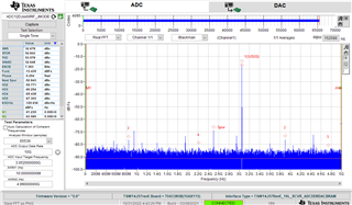
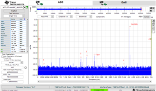
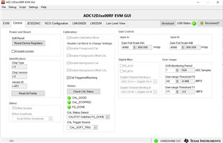
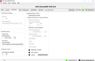
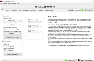
We do know that the clock/4 spur we see on our setup measurement is due to something related to the ADC interleaving and calibration or something related & we feel that there, most likely, has to be a way to get rid of it. We have tried the calibrations available, used two different boards, and so on. There are a bunch of JMODEs and quite a number of bells and whistles and I do not claim to understand them all. For example, different JMODEs are there letting you use different reference clocks and ADC modes. There are background and foreground calibrations which we have played around with... There are other settings specific to the ADC and others to the clocking skims... We are still, as we go on evaluating it, playing around with it as well as actually use it for projects and some production related tests in our labs. What is bugging me is why I couldn't get rid of this clock/4 spur I am seeing with this configuration for example. In this setting I am using JMOD1, DEVCLOCK=10GHz/2=5GHz, REFCLK=5GHz/20=250MHz, Input frequency is swept DC to Nyquist, tried both background and foreground calibrations, etc. Attached are some setting example captures as well as HSDC-Pro UI captures.
Has anyone doing something similar and coming across the 10GHz/2/2=2.5GHz spur we are seeing? It feels like a calibration\ADC interleaving related thing... or are just not lucky and both boards bad HW wise? Or are we entirely missing something important?
Regards,
Mesfin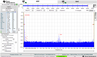

 .
.
