Other Parts Discussed in Thread: LMK00304, TPS22917
Hi expert,
I am new to ADC devices, and the customer has several questions about the device application, please kindly find below questions,
1. The output pins of ADC09xJ1300: D8+, D8-... What are the usage of these pins? How to distinguish the four channels of A,B,C,D, does the result of these channels output in turn?
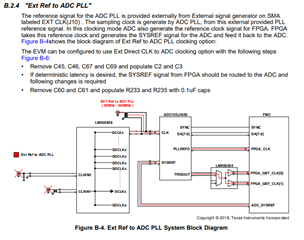
2. The customer wants to use the following reference design, can the 50MHz VCXO be removed and use the internal VXCO of FPGA?
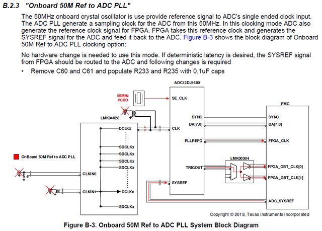
3. From the Figure B-3 above, can LMK00304 be removed? What does this do? What is the function of the other pins-SYNC, SYSREF, PLLREF0? What signals are required from the FPGA?
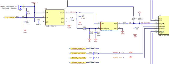
4. From the picture below, does the TPS22917 is a must if Y2 is always working?
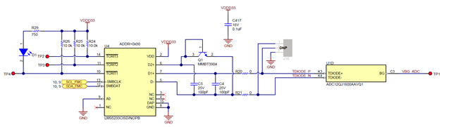
5. How does the Tdiode+/- work when the temperature is over target?
Thank you for your reply.
Best regards,
Bryce