This thread has been locked.

If you have a related question, please click the "Ask a related question" button in the top right corner. The newly created question will be automatically linked to this question.

ADS7038-Q1: ADC does not sample on configured port

Part Number: ADS7038-Q1
Other Parts Discussed in Thread: RM48L952

Hello,

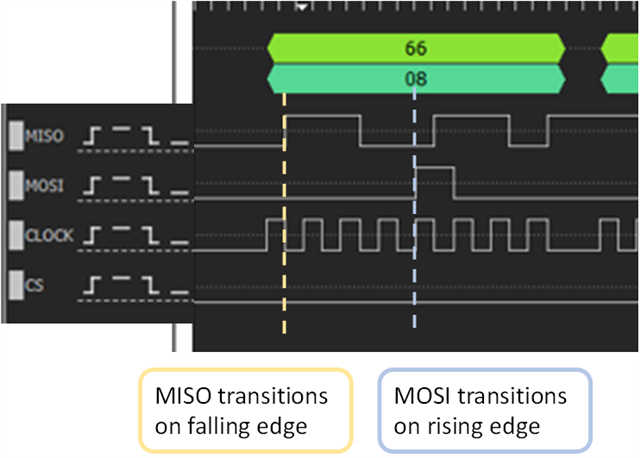
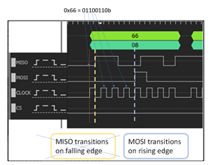
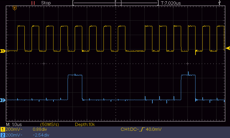
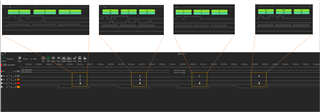
I have a custom board which embeds an external ADC with the part number described above. I want to read data from port 4 but all the time the read data belongs to port 1. Please find attached the SPI trace I use to read port 4 data.

Best Regards,

Cosmin Briceag

  • Cosmin,

    I will review your digital waveforms and provide some advice by Monday morning.  

    Thanks, Art

  • Hello Art,

    Did you get the chance to have a look on my issue ?

    Best Regards,

    Cosmin

  • Cosmin,

    This device has programable SPI protocols for configuring the device (see table 8.8).  Which mode are you using?  It appears to me that you are treating MISO and MOSI differently from a mode perspective.  Both of these signals should be captured on one edge, and should transition on the opposite edge.  In your case, MISO transitions on the falling edge and MOSI transitions on the rising edge.  I think if you rectify this discrepancy you may resolve the issue.  See picture below:

    I hope this helps.  Sorry for the delay.

    Art

  • Hello Art,

    In my opinion (please correct me if I'm wrong) the sampling on MISO hapens on rising as well. This is the default configuration for DATA_CFG register. Moreover, I overwritten it with 0x00 (SPI mode 0).

    By the way, I couldn't find table 8.8.

    Do I have to do something preliminary before starting to interogate the device for its inputs? By the time being I do the following in startup phase:

        setRegisterBits(SYSTEM_STATUS_ADDRESS, SYSTEM_STATUS_BOR_MASK);
    
        setRegisterBits(GENERAL_CFG_ADDRESS, GENERAL_CFG_CH_RST_SET_ALL_CH_AS_ANALOG_INPUTS);
    
        writeSingleRegister(SEQUENCE_CFG_ADDRESS, SEQUENCE_CFG_SEQ_MODE_MANUAL);
    
        writeSingleRegister(DATA_CFG_ADDRESS, 0x00);

    Thank you,

    Best Regards,

    Cosmin

  • Cosmin,

    1.  Sorry, I meant table 8-8 on page 24.

    2.  In general, for SPI both MISO and MOSI sample data on the same edge.  Both also transition the data on the same edge.  In your case MOSI transitions on the rising edge of the clock.  This is also the edge for mode 00 that the signal is captured on by the ADC (slave).  Depending on delays, setup time, and hold time it is not certain what the logic state is.  The master should transition the data on the falling edge for mode 00.  Below I show and example of typical mode 00 communications, and invalid mode 00 communications where the master transitions data on the rising edge.

    3.  I suggest you do a register write followed by a read to confirm that you have SPI configured correctly.  I think that once you get SPI communications correct, you will not have the issue where you get the wrong input (port).

    I hope this helps, Art

  • Hello Art,

    Thank you very much for your patience. 

    It is really odd because my uC (RM48L952) is configured with SPI-00.

    I managed to put the uC in 01 and now it seems I have the waveform you described (the good one). Please find attached. But for unknown reason the device does not send anything back. I will investigate, but at least now I have the proper waveform. 

    Thank you,

    Best regards,

    Cosmin Briceag

  • Cosmin,

    This looks correct now.  Note that the definition of what SPI modes are is not consistent for all devices.  I'm not sure why the device doesn't send anything back.  Do you mean that SDO is constant high or low?  It sounds like you are still in the debug stage so let me know how your investigation proceeds.  

    Art 

  • Hello Art,

    I got it functional. Thank you very much for your professional support.

    Best Regards,

    Cosmin