This thread has been locked.

If you have a related question, please click the "Ask a related question" button in the top right corner. The newly created question will be automatically linked to this question.

THS1206: Read/Write Timings and pin selection

Part Number: THS1206
Other Parts Discussed in Thread: THS4521, ADS1278

Hi,

I am programming and reading from THS1206 ADC using Verilog. The final use of this ADC would be for piezo sensor. Currently, on the board all the defaults are considered as per the datasheet. There are few things those are not mentioned as listed below:

1. Can I tie the pins CS0 and CS1 permanently to GND and VDD respectively? If so, what are the potentials to be used (nominal 0V and 2.5V I feel)?

2. To read the data for a single differential channel (AINP, AINM) (others not used) with TL = 1, CONV_CLK = 6MHz, DATA_AV = active low pulse, VREF = internal, continuous conversation mode, sensor not connected yet:

What should be the time interval between RDbar and DATA_AV active (since datasheet says to read after DATA_AV active but before falling edge of CONV_CLK)?

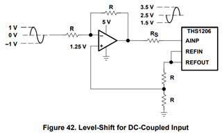
3. What should be the minimum input range for the above specs (both the inputs are clamped using DC Clamping circuit present on page no. 36)? Is it possible to read when I short/open the input terminals?

4. If I do not clamp, is it possible to realize the noise behavior/ENOB/Noise free bits with shorted inputs?

5. While configuring the CRs should there be any time gap required? Can I send config word in consecutive clocks?

Thanks

  • Hi Prakash,

    1. Yes - you can hold /CS0 and CS1 static on the THS1206 so long as there is nothing else sharing your data bus.
    2. Ideally you would use DATA_AV as an interrupt.  You need time to fill the pipe, so there are 7+TL  conversions before you will see DATA_AV, you should it go low after the eighth CONV_CLK and then toggle with every clock there after.
    3. I'm not sure which DC clamping circuit you are referring to, but yes, you can short the inputs and do a conversion.
    4. Yes
    5. You only need to worry about the setup and hold timings for reads and writes, no other delay is required.
  • Hi Tom,

    Thanks for the response.

    1. Nothing is shared on the bus. Ok, I will use as per your suggestion.

    2. Sure.

    3. This is the one I am discussing about:

    In my design both AINP and AINM are clamped using the same circuit. If is the case, what should be minimum input range? I tried shorting those inputs to check the output which showed all bits 0s. Is that correct? Don't I get any noise response?

    4. How many noise free bits will there for shorted input?

    5. Setup and hold times are taken care.

    Thanks

  • Ah!  OK - DC Coupled, Fig 42, that circuit is assuming a single ended setup.  Where are you shorting the inputs?  How are the CHSELx bits configured?

  • Hi Tom,

    It's the reference circuit shown. I am shorting inverting terminals of opamps. CHESELx bits are configured as AINP & AINM differential ie. CR0 programmed as x020 while CR1 is x410.

    What will be an output when I short opamp input terminals (inverting terminals)?

    What will be an output when I remove this DC Coupled clamping and short AINP & AINM?

    What I had observer without input clamping circuit and inputs shorted was 0. When I added input White Noise between AINP & AINM then also output was 0. But when this noise was DC clamped by 1.5V, then bits started toggling.

    Would you let me know on this behavior?

    Thanks

  • Hi Prakash,

    Shorting the OPA inputs, or AINp/AINn, directly should result in a differential input of 0V, which would give in turn a 0V output conversion result.  Can you provide screen shots of the VIN with the 'DC clamped by 1.5V'?  Are you essentially putting a common mode offset on the inputs in that case?

  • Hi Tom,

    Oh! So for 0V input/inputs shorted will have 0V output. If that is the case then, what should be the minimum input value?

    I am sorry for schematic since I generated noise from signal generator and added a battery (AA) physically between input of ADC and output of generator.

    Thanks

  • Hi Prakash,

    As noted on page 3 of the THS1206 datasheet, the differential input of the device is limited to 2V.  The common mode input in differential mode is usually set to 2.5V so that the inputs can swing +/-1V around the common mode input level. This is described on page 35 of the datasheet.

  • Hi Tom,

    I do agree to you. If my input is swinging between ±0.5V then what should be the clamping level? What will be one LSB value?

    Thanks

  • Hi Prakash,

    You could use the circuit of Figure 42, just change the gain to 2 so your full scale input matches that of the THS1206.  LSB size is FSR/2^N.

  • Hi Tom,

    Can I use that circuit in differential mode?

    Thanks

  • Hi Tom,

    Thanks for the reference. I just needed to know if I can you the circuit for differential input since the device that I am connecting is already a differential one. So, no need to further change the input into differential.

    Thanks

  • Figure 42 is for a single ended sensor.  If your sensor has a differential output signal and you want to use the single ended input option of the THS1206 you would need to use a difference amplifier with a common mode input to level shift the signal.  Thank a look at this app note for a reference:

    https://www.ti.com/lit/an/sbaa229a/sbaa229a.pdf

  • Hi Tom,

    My sensor has differential output. And I wish to use differential ended only not single ended. Would you suggest me on this?

    Regards

  • Take a look at the THS4521.  The circuit on the first page of that datasheet shows an interface to the ADS1278.  Using the THS1206, the REFOUT pin would connect to pin 2 (the Vocm input) of the THS4521. 

  • Thanks Tom.

    Does the data get written to FIFO on falling or rising edge of CONV_CLK? Since I have datasheets one says falling edge other rising edge.

    Where do find the timing related information like set-up and hold-time, minimum timing requirements for read/write operation? Since, DRDY sometime pulses other time it doesn't.

    Thanks

  • Hi Prakash,

    This app note may help: Designing with the THS1206  If you sometimes see DATA_AV and sometimes not, that is normally caused by failure to properly read all data out of the device between DATA_AV strobes, or not waiting for the appropriate 7+TL initial pipe delay.

  • Hi Tom,

    Based on that document I wished to know:

    Whether the data get written to FIFO on falling or rising edge of CONV_CLK?

    Other timing specs like after/before rising/falling edge of CONV_CLK how the read/write should be taken care are not listed in the document.

    Regards

  • Hi Prakash,

    In continuous conversion mode, the sample is converted on the falling clock edge and then written to the FIFO on the rising clock edge.  The read and write timings are based on combination logic.  If you are holding CS0 and CS1 static, the read cycle would be similar to Figure 38 (ignoring the CSx setup and hold times).

  • Hi Tom,

    The document you shared have above statement. It 's confusing since according to other datasheet or according to you contradicts this. So only asked about the FIFO.

    During the read operation what I have observed is, I have to wait until DATA_AV rises to 1 then only I can send read signal low. I am trying to reduce the period of DATA_AV being low by asserting read signal after the falling edge of DATA_AV, but it not pulsating only. And other aspect I noticed is, read signal assertion should either on rising edge or falling edge of CONV_CLK after DATA_AV goes low (Note: CS0 and CS1 are static). Datasheet says to read after DATA_AV goes low, but how much time after?

    Would you clarify on these issues?

    Regards

  • Hi Prakash,

    Yes - it can be a bit confusing initially.  There are two conversion modes with the TS1206, please see the 'Conversion Modes' section on page 16 of the datasheet.  The DATA_AV signal is also programmable to be active lo/hi and pulse/static. By Figure 38, since CSx is static, once /RD is asserted you have a max delay (ta) of 10nS, the data would be strobed to your CPU on the rising edge of /RD (min 10nS later).

    So lets start again with you telling me what is written to the configuration registers CR0/CR1.  If you can include an logic analyzer trace showing your CONVST, DATA_AV, /RD, /WR that would be great!   

  • Hi Tom,

    I do agree and I had programmed DATA_AV as lo, pulse.

    Registers configured as: CR0 = 0x020, CR1 = 0x410. I will add logic analyzer results in next mail since my board is unavailable.

    Regards