This thread has been locked.

If you have a related question, please click the "Ask a related question" button in the top right corner. The newly created question will be automatically linked to this question.

ADS1278: Design Inquiries

Part Number: ADS1278
Other Parts Discussed in Thread: OPA2350, , THS4521, OPA350, REF5020

Hello E2E Experts,

Good day.

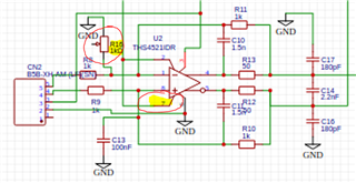
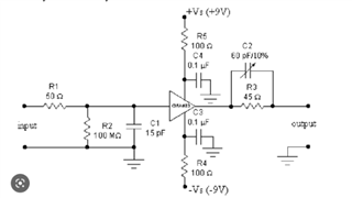
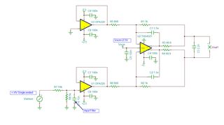
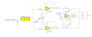
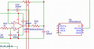
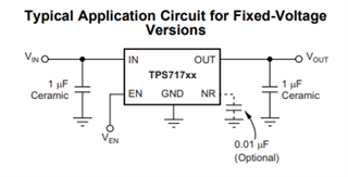
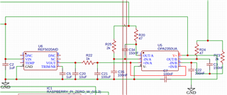
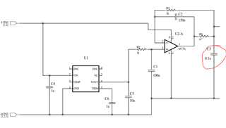
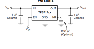
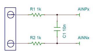
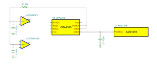
Does the datasheet on page 39 include the anti-aliasing design? Because I'm trying to use its analog engineer's calculator to design it,
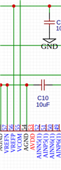
and I added some resistors and capacitors based on this design, is it working?
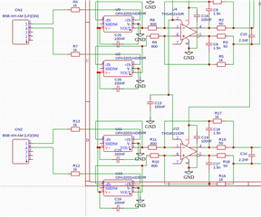
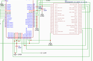
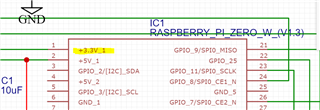
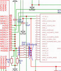
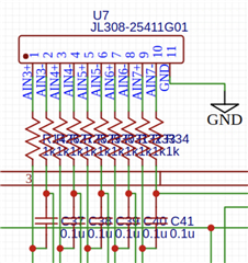
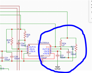
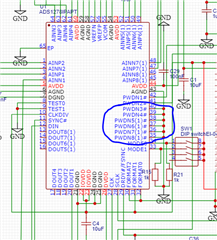
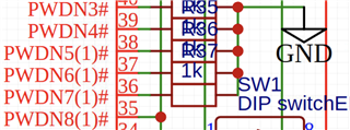
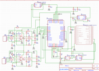
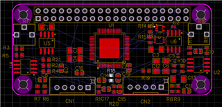
I also have my PCB layout with this email, please feel free to take a look by the way.
Thank you in advance.
Regards,
CSC
  • Hello,

    Yes, the example input amplifier circuit on page 39, Figure 89, not only drives the ADC input, but also performs as an antialiasing filter.  Assuming the CLK frequency is 27MHz, it will provide better than 55dB of attenuation for any input signals in the fCLK/4 band.

    There are a few schematic errors for the input amplifier.

    1. Pin 7 is the power down pin.  It should either be left floating or connected to the +5V supply, pin 3.

    2. Resistor R16 should not be included.  This will cause an unbalanced differential signal and will not perform as expected.

    3.  The reference should use a buffer circuit for best performance.  U2-A in below is OPA2350.

    4.  There are many missing pin connections on the ADC.  All digital inputs need to be connected to IOVDD or GND depending on desired functionality.  The external thermal pad EP, pin 65, needs to be connected to ground.

    5.  Regarding the layout, all power supply bypass capacitors, reference capacitor, and input capacitor should be placed as close as possible to the ADS1278 pins to provide good performance.

    6.  For layout, a single ground plane is recommended.  All ADS1278 ground pins (AGND and DGND) as well as the thermal pad, should be connected to the same ground plane directly beneath the ADS1278 package for reliable performance.

    It appears the customer is using Frame Sync.  If the host processor does not support this type of interface, it can be difficult to get it to work.  If the maximum data rate needed in the design is 105kSPS or lower, I suggest using SPI mode, which is supported by all processors.  In the case of SPI, the CLK frequency can be set to 27MHz.

    Once the customer has updated the schematic, please send updates and I will review.  Also, please confirm with customer what maximum sample rate is needed in their design.

    Regards,
    Keith Nicholas
    Precision ADC Applications

  • Hello Keith,

    Good day.

    I just follow as your way to edit my circuit, but there have some issues that I need to discuss with you:
    First, for the second part of the R16 resistor, I add this because my sensor input range does not fit to ADC input,
    The sensor I used is Capacitive Accelerometer (as shown in the figure), and its input range is +6V to -6V or higher.
    So that the reason I add a variable resistor to fitting in general purpose sensor.
    I also think it may cause some problems of frequency response, Would you have any suggestions?
    Second, it's about the SPI driver, I would like to know if it really need RTOS or not for my case,
    because I didn't build RTOS into my RPi zero already.
    And here is what I edited recently (the number is follow as yours):
    1. Pin 7 is left floating. Is it will be better that pull it to Vdd could prevent the leakage current?
    3. Add a buffer circuit before input of VREFP and VREFN
    4. I connect PWDN pin 3~7 to the GND, but I didn't change the PWDN1 and PWDN2. (I'm not pretty sure if I misunderstanding or not)
    # The problem 5 and 6 will add into my layout after the whole circuit design is done. (I think I would rebuild place and route of it ) #
    7. I set FORMAT[2:0] = 010 as discrete data output SPI mode.
    For my purpose sampling rate of sensor, I am consider it to be 200 Hz~1000 Hz (200 Hz is enough for us)
    The update schematic is following as this mail, please check it if you are free.
    And I also providing my design project, the design tool I used is EasyEDA.
    The project website:
    Below is the schematic:
    Regards,
    CSC
  • Hello,

    I will review the updated schematic by end of business this week.  The changes described should work well.  There should not be any problems leaving pin 7 of THS4521 floating; this pin is internally pulled high to default to power-up state.

    An RTOS is not required, but you should use an interrupt routine to monitor the DRDY output signal of the ADS1278.  Trigger the interrupt routine on the falling edge of DRDY, and then clock the data out of the ADC as needed.  You can use FORMAT=010, but you will need separate SDI inputs on your processor.  Since you are operating at a low data rate, 2000sps or less, I would suggest using FORMAT=000, which will send all data on a single SDO line.

    Regarding R16, the best way to accommodate different sensor output ranges is to add some additional buffers.  I will provide a suggested input circuit when I review the updated schematics tomorrow.

    Thanks,
    Keith

  • Hello,

    Since this is an IEPE data acquisition design with two channels, I suggest looking at the new TI Reference Design for IEPE sensors.  

    TIDA-010249, Four-channel synchronous vibration sensor interface reference design

    Although this design supports 4 channels, it can easily be modified to support 2 channels as well.  It includes a user's guide with schematics and suggested board layout.

    Regards,
    Keith

  • Hello Keith,

    Good day.

    Does it mean the whole circuit could work as I thought with this design (by default input range of the ADS1278)?
    because it still has some floating on ADS1278, just want to make sure about it.
    For the last mail before it, page 39 is already applied anti-aliasing filter design, but I also use the ti calculator to add another filter on the input driver.
    Should I remove it? I think it might be useless to add this filter.
    The second part of RTOS, does it mean that I need a monitor mechanism to check the state of DRDY?
    My idea is to pull DRDY to RPi GPIO and add this value to the driver program with if else to get it state.
    This project's purpose is to make it into a black box and throw it underwater, so we could only check the data after the measurement is done.
    And about FORMAT mode = 000, does it mean that the ADS' sampling rate is high enough to get data like parallel input with this mode?
    Because it looks like ADC reads a channel's value per 24 cycles and then reads the next channel on page 32.
    For the variable of the input function, do you mean that I could change the amplifier gain to reduce the voltage of the sensor?
    For example in the following picture, I could change the ratio of R1 and R2 to achieve it.
    Would you have any recommendations for it?
    Regards,
    CSC
  • Hello,

    The input amplifier for the ADS1278 can convert a +/-6V single-ended input to the full scale input range of the ADS1278, which is +/-2.5V differential.  Below is a circuit that can accomplish this.

    If you are using the Silicon Labs sensor, the output is already differential, and produces a full scale output of +/-4V differential with a common mode of 2.5V.  If using this sensor, then the below circuit will scale the output correctly.

    The sensor is limited to 2kHz of bandwidth.  You can add a single capacitor at the first stage amplifier input to create an additional low pass filter, which should provide more than 80dB of attenuation of any aliased signal.

    Yes, for the digital communications, you must monitor the state of the DRDY pin.  When this pin goes low, it indicates that the conversion result is complete and the host processor should read the data.  If you processor is fast enough, you can poll this pin, or more typically, use a hardware interrupt.

    When using FORMAT mode = 000, data for all channels will be output on DOUT1 pin.  Please refer to Figure 79 for more details.

    Regarding your schematic design, below are several corrections that should be made.

    1.  For the reference pins, add an additional 10uF cap directly next to the ADS1278 VREFP and VREFN pins.

    2.  U5 can be replaced by the additional channel in U8.1.  OPA2350 is the 2 channel version of the OPA350.

    3.  Add a 0.1uF power supply bypass capacitor to all IC power pins, including U8 (pin 8 to pin 4), U5 (pin 7 to pin 4).

    4.  Add 0.1uF power supply bypass capacitors to each of the ADS1278 AVDD power pins.

    5. The SYNC pin11 should be connected to an IO pin on the host processor.  This pin can be used as a RESET function for the device, and should be toggled by the processor after the power supplies are stable.

    6.  Because you are using SPI mode, you can eliminate U7 and U3.  These additional parts are only needed when operating in the highest speed frame-sync mode.  DOUT1 can be directly connected to the MISO input of the host processor.

    7.  DVDD, pin 26, is an internal digital supply for the ADS1278.  This pin must be supplied by a regulated voltage source.  Please add an additional power supply use a linear regulator to generate a stable +1.8V supply.

    8.  CLK, pin 27, needs to be a continuous clock.  The specific frequency of this CLK depends on the output data rate and desired mode of operation.  If operating in high speed mode, then setting this clock to 27MHz will result in an output data rate of 105ksps.

    9.  DRDY pin 29 needs to be connected to the host processor.

    10. AVDD pins 44 and 53 need to be connected to the +5V supply.  A 0.1uF supply bypass capacitor for each of these pins should also be added.

    Regards,
    Keith Nicholas

  • Hello Keith,

    Good day.

    I really appreciate to your supports, and I am trying to learn about those informations.
    I'm sorry about that I late too many days for update my project.
    I was edited my circuit follow as your suggestion.
    And I would like to explain step by step.
    The first change of the input I add the buffer circuit under the differential input design.
    Next is about the corrected:
    1. I add the 10uF bypass the VREFP and VREFN.
    2. Here I have a question, is that I need to change the IC to the two channels(OPA2350UA) then connecting another channel to VCOM?
    3. For all OP amplifier, I add the 100nF capacitor bypass their voltage supply (V+ / V-).
    4. And also all AVDD are bypass a 100nF.
    5. I pull the #SYNC (pin11) to GPIO26(RPi_pin37).
    6. With SPI mode, I pull the DOUT1(pin20) to SPI0_MISO(RPi_pin21).
    7. To simplify the circuit, Could I pull the DVDD to the RPi +3.3V to 1.8V with a divider?
    8. I pull CLK and SCLK to SPI_SCLK(RPi_pin23), Of my concept is follow the clock from RPi. Is that right?
    9. I pull DRDY to the GPIO25(pin22).
    10. I pull the AVDD(pin44) to +5V and with a 100nF bypass.
    Currently my progress, and the circuit is looks mess a lot than the before.
    I'm sorry about that I would take you many time to answer my question and review my circuit.
    I also update the circuit on website (but PCB didn't update yet).
    I look forward to your response, and thank you so much.
  • Hello,

    Keith is on vacation now, please allows a response delay from him.

    Best regards,

    Dale

  • Hello,

    The input buffer circuit looks correct.  There is one error; the shutdown pin 5 for the OPA320S devices must be connected to V+(pin 6) in order to enable the amplifier. Pin 5 (SHDN) connect be left floating

    • (2)You can use two separate OPA350 amplifiers for U5 and U8, or you can use a single dual amplifier, OPA2350, which is the two-channel version of the OPA350.
    • (7) No, this is a supply voltage that needs to be driven from a low impedance source.  Use a 3.3V->1.8V linear regulator to provide this supply voltage.  There are many different regulators that can be used; TPS71718 is a good example.    
    • (8) CLK must be a continuous clock.  SCLK using SPI is typically a start-stop clock, only active when transferring data over the SPI port.  I suggest using a separate clock oscillator for the CLK source, such as HX2127002Q or similar.

    Everything else looks good at this point in the design.

    Regards,
    Keith

  • Hello Keith,

    Good day.

    The change would update until next Monday (1/9), please allowed me to take some time to review those corrections.
    Besides, I have some concerns with the data acquisition of ADS1278:
    In our case, we use the sensor SDI 2XXX-XXX (we didn't make a decision on the sensor type yet),
    I am thinking about the input sampling rate of ADS1278, I am still concerned that the actual sampling rate is uncertain.
    the formula I refer to is Fs = (clock frequency) / (2 ^ resolution),
    if the sampling rate is following this equation, the actual sampling rate might not be sufficient for our purpose.
    Is there any suggestion? Because I am too weak in this domain of knowledge (maybe I misunderstood).
    Regards,
    CSC
  • Hello,

    Using a 27MHz clock, (Pin 27 supplied with a continuous 27MHz clock), the output data rate in High-Speed mode (pins 33 and 34 connected to ground) will result in an output data rate of 105.469ksps.  This output data rate determines the bandwidth of the digital filter, which is equal to 0.49 of the data rate, or:

    f-3dB=105.469*0.49=51.7kHz.  The maximum bandwidth of the SDI sensors appears to be less than 4kHz, so you have more than 10x the bandwidth needed for these sensors.

    Based on the latest version of the schematic, I see that the SCLK and CLK pins are tied together.  These pins should be separated, and a 27MHz clock oscillator connected directly to the CLK pin 27 of the ADS1278.

    Regards,
    Keith

  • Hello Keith,

    Good day.

    I review your e-mail and finish the circuit correction, Here are the following edits:
    1. OPA320S, the buffer to analog output, I set the pin5(SHDN#) to V+ to enable the buffer.
    2. I use OPA2350 to make two buffer to VREFP and VCOM, but here I have a question of it, could +IN/A and +IN/B use the same source from U6 (red wire)?
    3. Supply voltage of CLK and DVDD are built by TPS71718, I review it's datasheet to connect pin4(FB) as following picture, and pull the VDD to the RPi +5V, Does the +5V voltage should provided by addition battery or other source?
    4. And clock source to ADS1278 are built by HX2127010Q, VDD also connect to the source from TPS71718.
    Sorry my schematic has becomes a lot more complicated.
    But I also worry about the total power consumption would be too high to RPi, does it needs another power supply module for this ADC circuit?
    You can review this and previous e-mails without putting too much pressure on response time.
    Regards,
    CSC
  • Hello,

    1.  Looks correct.

    2.  Yes, the +InA/+InB can be connected to the same node in the circuit.  Each of these pins are high input impedance and will not load the output of the RC filter (filtered version of the reference voltage).  However, it looks like you have a schematic error.  C35 should be connected on the other side of R25.

    3.  TPS71718 is the fixed 1.8V output version of this device.  You do not need to connected an external resistor network to the FB pin.  In fact, pin 4 for the TPS71718 is a noise reduction (NR) pin, and can either be left floating or connected to a 10nF capacitor to ground to further reduce noise.

    You will need to estimate total current requirements and determine an appropriate power limit for your system.  I would budget at least 100mA for the 5V supply.

    4.  The clock oscillator needs to be powered from the same supply voltage as connected to IOVDD.  In your case, this clock oscillator needs to power from the +3.3V supply.

    Regards,
    Keith

  • Hello Keith,

    Good day.

    I was reviewed previous e-mail, and I edited the circuit of your suggestions,
    First, the clock oscillator that I use does not same as your suggest because there has no HX2127002Q in there library.
    And I replaced it to HX2127010Q, that why I pull supply voltage to +1.8V.
    And I would like to add a screw terminal if there has the free space on PCB board, could I just pull the pin from ADC to terminal (just want to left some channel to use)?
    Another issue that I concerned is about number of sample, Is there any method could estimate data per second?
    Of my purpose, If I set time sleep as 5ms in my program, the data output would be 200 data per second in the csv file (consider that bandwidth of SPI is wide enough).
    In the data sheet, It shows that data output rate is 144ksps under high speed mode.
    but I think it would not be easily to realized this performance, Is it possible?
    I hope that you could check my circuit, and if there has nothing error encountered, I would start to PCB layout.
    Regards,
    CSC
  • Hello,

    The output voltage of the clock oscillator must be the same voltage levels as the IOVDD supply voltage.  If you use a +1.8V clock oscillator, then IOVDD (and the digital signals from your processor board) must use 1.8V logic levels.  Based on your schematics, you have IOVDD connected to a +3.3V supply.  If this is the case, then the clock oscillator must operate from a +3.3V supply as well.

    The ADS1278 sets the output data rate based on the clock frequency (f-CLK), the CLKDIV level, and the MODE selection.  The maximum possible data-rates are displayed in Table 8.

    If you only need 200sps, then I would suggest using the Low-Speed mode (MODE0 pin34 logic high and MODE1 pin33 logic high), and reduce the CLK pin frequency as follows:

    f-DATA=f-CLK/2560 for Low-Speed Mode, CLKDIV=1.

    f-CLK=f-DATA*2560=200*2560=512kHz.  If you use a standard 1MHz frequency clock, then your data rate will be:

    f-DATA=1MHz/2560=390sps.

    In order to allow flexibility in the data rate, you may want to use pull-up and pull-down resistors for pins 33 and 34 to allow different speed mode configurations.

    The ADS1278 constantly converts data, pulling /DRDY pin29 low when data is ready to be read from the device over SPI.  The processor needs to monitor the /DRDY signal and transfer data after /DRDY goes low.

    Regards,
    Keith

  • Hello Keith, 

    Good day.

    I just reviewed the e-mail and edited the circuit.
    Is it possible to pull the oscillator IOVDD to +3.3V instead of +1.8V?
    It seems that the supply voltage number in the datasheet needs to be +1.8V, should I replace it with HX2127002Q?
    I found another oscillator with 27MHz and +3.3V, Is this available?
    I make a pull-down resistor to customize the operating mode.
    According to your saying, does that mean I do not need to worry about the sample per second issue of ADC?
    I hope that you could check my circuit, and if there is no error encountered, I would start with the PCB layout.
    and I are wondering about what if I want to make a set of screw terminals to extend the input?
    Should I pull AINP and AINN to the terminals to make it also use a single /differential type?
    Thank you for your continuous support with this thread.
    Regards,
    CSC
  • Hello,

    Yes, any clock oscillator specified for +3.3V operation that provides a CMOS output can be used.  HX2127002Q or HSO321S_27MHz can be used.  The ADS1278 controls the data rate based on the f-CLK frequency, and the CLKDIV and MODE pin settings.

    If you want to use the unused ADC channels, you will need to enable them by connecting the PWDNx to +3.3V.  For any unused channel, I suggest adding an RC filter between the screw terminals and the AINPx and AINNx inputs.

    Below is my review of your schematic:

    1.  Adding R15 and R21 as pull-down to the MODE pins and the dip switches is correct.  However, the DIP switch needs to connect to the +3.3V supply, not the +5V supply as you have drawn in your schematic.

    2.  The clock oscillator OE pin 1 should either be connected to VDD (+3.3V) or left floating to enable the output of the oscillator.

    3.  ADS1278 AVDD pin 44, REF5020 VIN pin 2, and OPA2350 V+ pin 8 need to be connected to the +5V supply.  Your schematic just has these connected to each other, but not to the +5V supply pin from the processor board.

    Regards,
    Keith

  • Hello Keith,

    Good day.

    I already correct my circuit as the last following support.
    I changed the oscillator to HSO321S_27MHz to replace the original ones, and correct the wire connection.
    Besides, the screw terminal connection from AIN3 to AIN7 is done already with the RC circuit and corrects the misconnection of +3.3V.
    You would see the correction on the project website: https://oshwlab.com/middlehuang/adc_input_test
    if there have any problems with my circuit, please let me know.
    I look forward to hearing from you, thank you very much.
    Regards,
    CSC
  • Hello,

    The VCOM buffer is connected incorrectly.  VCOM pin55 on the ADS1278 is an output, and should be buffered by U5B, and then drive the Vocm pins of U4 and U12 (THS4521).

    Here is the correct schematic connection:

    Also, if you want to use the extra channels, AIN3.....AIN8, then you need an option to power-up these channels.  Your current schematic has channels 3 through 8 powered down by connecting PWDN3 through PWDN8 pins directly connected to ground.  I suggest adding pull-down resistors (1kohm to ground)  to each of these digital inputs so you have the option to power these channels ON at a later time.

    Regards,
    Keith

  • Hello Keith,

    Good day.

    I correct the circuit as per your following mail.
    Does it mean that VREF and VCOM should not use the same source from OPA2350UA (OUT/A) because of high impedance?
    I also add the pull down resistors for each PWDN.
    But I have a question about it, how could I switch ON those channels that connected to the 1k ohm to ground?
    Does it means that I need another switch to connect to GPIO to those pin?
    If there has any incorrect with this circuit, please let me know.
    I hope that I could get into the next step to drawing layout diagram. (because I am wondering to graduate as soon as possible ( :
    I look forward to hearing from you, thank you.
    Regards,
    CSC
  • Hello,

    The VCOM pin on the ADS1278 is an OUTPUT signal.  It is a high impedance output, which is why it needs to be buffered using an amplifier.  The output of the amplifier then drives the VOCM INPUT pins on the THS4521 amplifiers.

    Your schematic updates look correct.  The PWDN pins need to be connected to IOVDD (3.3V) if you want to enable those channels.  By adding the 1k pull down resistors, the channels will default to off, but if you remove these and add a jumper to the PWDN pin and IOVDD, then you can enable these channels.  If preferred, you can add another switch like you did for the MODE pins to easily enable these channels.  Another option is to connect these pins to unused GPIO channels on the RPi board, similar to what you have already done for PWDN1 and PWDN2 pins.

    Regards,
    Keith