This thread has been locked.

If you have a related question, please click the "Ask a related question" button in the top right corner. The newly created question will be automatically linked to this question.

ADS7038-Q1: AINx input impedance

Part Number: ADS7038-Q1
Other Parts Discussed in Thread: ADS7038, TLA2528

Hello,

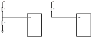
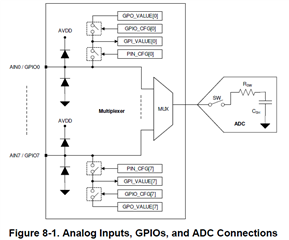
What is the input impedance of AINx pin?

I need to monitor the voltage using ADC and I'm adding 1kohm before the ADC pin to limit current.

Can i know input impedance of ADC input pin so that I will get a clarity on how much voltage is dropped across 1kohm.

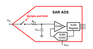
Also, can i know AINx pin capacitance, MUX resistor and MUX capacitance value?

Can i also know what is the relation between AINx pin input impedance and RSW (and MUX resistor if known)?

  • Hello

    The ADS7038 is a SAR ADC, which means it uses a switch capacitor circuit to measure the input voltage. This then means that the input impedance of the ADC is dynamic, as it is a switching capacitor circuit and depends on the switching frequency of the circuit. 

    If you share what your application is, and requirements, we can help you design the input circuit. 

    Also, there is a video series that provides background information as to how to drive a SAR ADC

    TI Precision Labs: Analog-to-digital converter (ADC) drive topologies (5)

    Regards

    Cynthia

  • Hello,

    Let us consider two examples.

    In the figure one, let's say I'm giving 2V with voltage divider, the effective voltage across the AINx pin will not be 1V right? Because, RSW is 150ohm and it is parallel with 1k which is connected to GND. The effective resistance will be 130ohm and voltage will be around 0.3V.

    In figure two, I'm connecting 2V with 1K series. The voltage across 1K will dropped more and we will not get exactly 2V across the AINx pin right?

    Of course both figure will have some value of capacitor and act as RC filter before the AINx pins.

  • I think the best way to show this is through a TINA Spice simulation.

    Please see attached file below. the simulation uses the TLA2528, which is an equivalent of the ADS7038

    To answer your questions directly, the first figure result in an ADC measurement close to 1V, and the second will measure 2V

    I would suggest watching the following training video, the slides are also available for download to review at your pace. It will explain how the sample hold circuit operate.  SAR and delta-sigma: Basic operation

    I will point out that this device uses the same topology as shown below, the datasheet does not show this diagram, though it would be helpful. The resister network connected to the ADC input is followed by the sample and hold switch, not the R_SW (in this diagram shown as R_SH). 

    Note that for these type of measurements, DC inputs without op amps, the sampling rate tends to be slower as the DC source would need to drive the ADC input. 

    Also, there are design circuits by use case/application available in: Data Converter Circuits

    The following may have some information that is related and helpful to your application: Monitoring NTC Thermistor Circuit With Single-Ended
    ADC

    ADS7038 Voltage Divider.TSC

    Regards

    Cynthia

  • Hello,

    So first figure result in an ADC measurement is exactly 1V, and the second will measure exactly 2V? Or will there will be less value?

    Also, what is the pin capacitance across AINx pin?

  • Vishwas,

    I will add a few comment to what Cynthia is saying.

    1. Once the internal sample and hold circuit is fully charged, the impedance of the input is very high for SAR converters.  Depending on the SAR there may be some small leakage (usually nA or less).
    2. You should not really think of the "input impedance" when connecting signals to the input of the SAR.  Rather, think about fully charging the RC circuit.
    3. The error introduced by not fully charging the internal sample and hold is normally called a "settling error".   Ideally, you want this settling error to be less than one half of one LSB.  This way the error is negaglible from the ADC perspective. 
    4. For voltage divider type inputs, the method to select components to achieve a good settling is relatively straightforward and is documented in driving-sar-without-amplifiers-video.  The video outlines a software tool that will help you choose the proper resistors, capacitors, and sampling rate for good settling. Note that a slower sampling rate allows more time for the internal RC sample and hold to charge.  Also, smaller external voltage divider resistors allow for faster charging of the sample and hold. 

    I hope this helps!  Please watch the video and see if that answers your questions.

    Art