This thread has been locked.

If you have a related question, please click the "Ask a related question" button in the top right corner. The newly created question will be automatically linked to this question.

ADS8166: Normal AD conversion values cannot be obtained

Other Parts Discussed in Thread: ADS8166

Dear Sir

1. Hardware schematic diagram using the ADS8166:

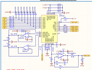
The input is eight 0-4.096V single-ended signals. The ADC is configured in pseudo-difference mode. The internal reference, reference buffer, REFBY2 buffer are enabled. The measured pin voltages of REFP (4.096V) and REFBY2 (2.048V) are correct. The pin voltages of DVDD (+3.3V),AVDD (+5V) and DECAP (2.8-2.9V, with slight differences among different chips) are correct.

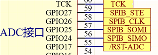
The following figure shows the connection between ADC and C280039CSPZ.

At present, normal ADC conversion results cannot be obtained, because DSP software engineers are not familiar with this kind of ADC register configuration and operation. I hope you can help to provide relevant technical support.

  • Hello Gabriel,

    When ADS8166 is reset or after power-up, the ADC should be reading the input voltage on channel AIN0.

    Please measure the voltages on the ADC-INP(17) and ADC-INM(20), and then verify the conversion result.

    Also, please ask the customer to capture a full SPI frame using either an oscilloscope or logic analyzer (/CS, SDO-0, SDI, SCLK).  /CS needs to be held high for a minimum of 2.5usec to allow the conversion process to complete, then take /CS low and send 16 SCLKs to transfer the conversion result over the SDO-0 pin.

    Regards,
    Keith Nicholas
    Precision ADC Applications