This thread has been locked.

If you have a related question, please click the "Ask a related question" button in the top right corner. The newly created question will be automatically linked to this question.

ADS7049-Q1: Rise/fall time calculation

Part Number: ADS7049-Q1

Hi

We want to find out the maximum possible input rise/fall time of ADS7049QDCURQ1. Therefore, we find out a TI application note. We understood that if we have the input transition rate and VIH(min) and VIL(max), then we can find out the rise/fall time using the following equation:

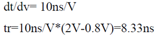
Here, VIH(min)=2V and VIL(max)=0.8V.

Is this approach correct?

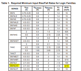
Also, in the TI application note, does the transition rate, (dt/dv) of SN74LVC mean 0.5ns/V. Please confirm.

Regards

Sreelekshmi.

  • Sreelekshmi,

    The SDO pin on the ADS7049 is the only digital output for the device. The minimum rise / fall time of the ADS7049 SDO pin is not specified.  However, the maximum clock rate of the device is specified and for proper operation of the digital communications the SDO pin will need to rise and fall in a fraction of this time.  The maximum clock rate is 32MHz (31.5ns).  For proper operation the SDO pin will need to transition in a fraction of this time.  

    Note that the actual rise time for digital signals will relate to the bus capacitance that they need to drive and so for longer trances with higher capacitance the rise time will slow. 

    Regarding the 5/10ns in the TI appnote.  You can confirm this with the logic team, but I believe this means 5ns rise time and 10ns fall time.  I didn’t see confirmation on this, but I don’t think you should device the 5/10 = 0.5.

    I hope this helps.  Can you elaborate on your concern?

    Art

  • Thank you for the response. Actually, we are performing signal integrity analysis, so we want the receiver specifications to compare the results and provide a judgement. CLK, SDIN and CS are the input pins of ADS7049. So, we want the maximum acceptable input rise/fall time of ADS7049. So, I was confirming that if there is input transition rate given in the datasheet, can we calculate the rise/fall time using the equation stated above.

    Regarding the 5/10ns in the TI appnote, I will confirm with Logic team.

  • Sreelekshmi,

    Regarding the maximum acceptable input rise/fall time (how slow can the signal rise):

    1. My comments were to estimate the minimum expected rise time (I edited my post to correct the comment).
    2. For slow moving signals you can have communications errors as the signal slowly transitions between a logic low and high.  Implications of Slow or Floating CMOS Inputs is a very good appnote on this subject.  It provides examples for different logic families.
    3. The max allowed rise time on digital signals is not specified for this device.  I will see if I can find an estimate of this value for you.

    Best regards, Art

  • Thank you for response. If you can find the estimate of the rise/fall time values, kindly update me.

  • Sreelekshmi,

    Based on Implications of Slow or Floating CMOS Inputs i think it will be at least 100ns.  I have some enquires with design / characterization to get a more precise answer, and will let you know if I find one.

    Art