This thread has been locked.

If you have a related question, please click the "Ask a related question" button in the top right corner. The newly created question will be automatically linked to this question.

ADS1299: Bias Amplifier filter and input filter questions

Part Number: ADS1299
Other Parts Discussed in Thread: ADS1298,
I have designed a functioning prototype using the ADS1299 ADC. I am digging into the bias amplifier and input filters at this time and need to understand 
a little more than what the datasheet provides. I will reference the ADS1299 datasheet SBAS499C revised January 2017, the evaluation kit user manual
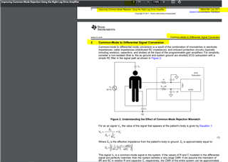
for the ADS1299 (EVK), SLAU443B revised January 2016 and the application note SBAA188 "Improving Common-Mode Rejection Using the Right-Leg Drive Amplifier" July 2011 I came across a few typos in the datasheet and app notes. If I'm incorrect, please let me know. In the datasheet section 10.2.2 talks about the gain set by Rbias although figure 73 shows this as Rf. I take it these are the same. In SBAA188 Figure 7 input filter capacitors show 47nF although the ADS1298 PDK schematic show 47pF. In ADS1299 datasheet, Figure 73 shows the input summing resistors as 220K. Equation 11 and nearby text refer to these as 330K. The ADS1299 can be set up to measure the bias amp input resistors itself. Set channel 2 ADC for shorted lead test with gain of 1 and enable BIAS2N and BIAS2P.
Connect channel 3 to BIASIN in bias measurement mode and enable the bias amplifier. Note that channel 1 BIAS1N and BIAS1P cannot be enabled with the EVK application,
likely a software bug. Read ch3 for Vout of the Bias Amplifier. The shorted lead test will bias the output to -0.25V on BIAS2N and BIAS2P, that is, it connects (VREFP + VREFN)/2 through a resistor to the programmable
gain amplifier (PGA) inputs. The inverting summing amplifier is Vout = -((Rf/Rin1) * V1 + (Rf/Rin2) * V2 ... ). The EVK has 392K ohm for Rbias (Rf) and the
bias output measured about 0.9V. Since all input resistors are the same, Vout = -(Rf/Rin) * (V1 + V2) and
solving for Rin = -(Rf * (V1 + V2))/Vout = (392Kohm * (-0.25V + -0.25V)/0.9V = 218K ohms. This is within 1% of 220K. So I take it equation 11 has the wrong value input resistor. Onto the questions I have. It is my understanding from datasheet 9.3.2.4.5, that the bias amplifier (or driven right leg - DRL), takes the common mode noise (CMN) from the PGAs,
amplifies it, inverts it and then feeds it back into the human body to further reduce the CMN. This is predominantly AC line frequency (50Hz/60Hz). It is a
closed loop system with the bias amp, human body/electrode model, input filters and PGA in the loop. The datasheet and SBAA188 app note only says the feedback
capacitor sets the bias amps bandwidth but there is no further explanation as to what the bandwidth should be set. Using fc = 1/(2*pi*R*C) it is set it to 106Hz
in the datasheet. The EVK has a gain resistor of 392K and Cf of 0.01uF (R8/C20) for a minimum DC gain of 1.78 and -3db cutoff at 40.6Hz.
For the bias amp to work properly shouldn't this filter pass the line AC frequency without attenuation and phase shift? If so, why is the EVK bandwidth lower
than the dominant CMN? I would appreciate a more thorough explanation of what the target bandwidth is for bias amplifier's low pass filter and reasoning
behind selecting that bandwidth. The next issue is determining the cutoff frequency of the input filters (Rfilt/Cfilt). From section 10.2.2
"The cutoff frequency for the filter can be placed well past the data rate of the ADC because of the delta-sigma ADC filter-then-decimate topology. Take care to
prevent aliasing around the first repetition of the digital decimation filter response at fMOD."
The goal is clearer here, you should have sufficient stop band at fMOD and above to band limit the input sample rate and provide sufficient passband
for the bandwidth of the output sample rate. You can derive from Table 1,2,3 in the datasheet that the bandwidth is approximately the output sample rate / 3.817.
The datasheet only shows 4.99K ohms and 4.7nF for input RC filter in Figure 74 example. This is the same first order input filter used on the EVK with -3db cutoff at
6.79KHz. It would have -47db attenuation at fMOD and the cutoff is well above the bandwidth for 16Ksps setting. If I was only going to use 250sps, could I
decrease the cutoff of the filter to improve the stop band attenuation at fMOD. Maybe or maybe not. In SBAA188 and in a blog "Three guidelines for designing anti-aliasing filters", there is an equation
CMR = 20 log ((Rtol + Ctol)/100) + 20 log(f/fc)
where fc is the cutoff of the filter and f is the CMN. SBAA188 goes on to say it may be better to have a larger bandwidth for the filter to improve CMR.
While I have found several instances in articles for that formula, I have yet found a derivation and theory behind it. CMR (CMRR) is the ratio of differential and common mode gain (or losses) in db. In the formula above, neither the tolerances nor frequency seem directly
related to the gain/loss of a filter stage and while 20 log(f/fc) could approximate the slope of the stop band for f > fc, it is not a model for
low pass filter gain. So if there is an in depth proof of this formula, could I get a reference to it? If not, could someone explain the theory behind it?

Thanks
  • Hi,

    We will need at least another 24 hours to get back to you.

    Thanks

  • Hi,

    Appreciate for the detail writing.

    1. "In the datasheet section 10.2.2 talks about the gain set by Rbias although figure 73 shows this as Rf. I take it these are the same. "

    That may be a typo, it should be Rf.

    2. "In SBAA188 Figure 7 input filter capacitors show 47nF although the ADS1298 PDK schematic show 47pF. "

    ADS1298 and ADS1299 are different devices, this document and figure are for ADS1298 not ADS1299. Also, that capacitor is something that people have option to change depending on the applications and experiments to configure the bandwidth, so it could be different if the document was done and release at different time of the EVM release.

    3. In ADS1299 datasheet, Figure 73 shows the input summing resistors as 220K. Equation 11 and nearby text refer to these as 330K. 

    Yes, this may be a typo.

    4.The EVK has a gain resistor of 392K and Cf of 0.01uF (R8/C20) for a minimum DC gain of 1.78 and -3db cutoff at 40.6Hz.
    For the bias amp to work properly shouldn't this filter pass the line AC frequency without attenuation and phase shift? 

    Ideally, The BIAS amplifier with the Cf serves as an integrator to either gain or attenuate & shift the noises to achieve some noise cancellation as well as provide DC bias to the unit under measurement(UUM) so that the UUM is not floating in an unknown voltage.

    The purpose of most RC on the EVM are provided for basic testing and evaluate. Customers don't need to stay with it, and can change those for their experiment and applications; they don't have to be exact the same way.

    For example, those two RC could be different depending how customer want to connect to the electrodes, and set the internal Rbias; different customers set/configure them differently depending on their applications&products.

    5."If I was only going to use 250sps, could I decrease the cutoff of the filter to improve the stop band attenuation at fMOD."

    Figure 74. is really just for example purpose, designers&developers can configure the filter differently and do tests&V&V and data collection&analysis for their interested signals and applications.

    6.

    "CMR (CMRR) is the ratio of differential and common mode gain (or losses) in db. In the formula above, neither the tolerances nor frequency seem directly
    related to the gain/loss of a filter stage and while 20 log(f/fc) could approximate the slope of the stop band for f > fc, it is not a model for
    low pass filter gain. So if there is an in depth proof of this formula, could I get a reference to it? If not, could someone explain the theory behind it? "

    Sorry, section 2 Common-Mode to Differential Signal Conversion is probably the info we can provide.

    Maybe you could take a look of the 

    "Winter, B.B. and Webster, J.G. (1983). Driven-right-leg circuit design. IEEE Transactions on Biomedical Engineering, Vol 30, No 1. Pp. 62 - 66."

    Thanks

  • Hi,

    Thank you for your timely comments,

    About the SBAA188 typo. please note that SBAA188 figure 7 expressly mentions  ADS1298EVM and the part didn't match however, this wasn't about the ADS1299, so my bad. 

    The reference to "Winter, B.B. and Webster, J.G. (1983). Driven-right-leg circuit design. IEEE Transactions on Biomedical Engineering, Vol 30, No 1. Pp. 62 - 66." was invaluable. It is behind a paywall but it was well worth it as it properly describes the bandwidth properly for the bias amp/RLD. In this paper, they use this feedback capacitor to compensate for the various delays in the system to prevent oscillation and prove their work.  The EVK filter loses close to 6db at the dominant common mode noise and would not effectively reduce that noise although it may serve to correct any DC offsets. 

    The reason for my queries is to understand the parameters around making design choice and not blindly copy the EVK. As I've discovered, that would be a bad idea. On the other had eval boards can serve as valuable additional documentation as long as one understands the goals and tradeoffs the designers made. 

    What do you mean by 

    section 2 Common-Mode to Differential Signal Conversion

    What document are you referring to? I see nothing in the datasheet or SBAA188 that matches that.

    There are problems with this formula.  I requested that TI show their work on how they arrived at it and whether the claim made that "keeping a large bandwidth"  maintains good CMR made by SBAA188 can actually be substantiated across all types of first order RC filters. 

    Perhaps you know of other documents which do a better job covering RC low pass filters in FDA and how it affects common mode rejection. 

    Bob

  • Hi,

    Glad the IEEE paper is informative.

    --------------------------------------------------------------------------------------

    "The reason for my queries is to understand the parameters around making design choice and not blindly copy the EVK"

    Comment: correct, EVK's purpose is not to be or for exactly copied and make into a product. Instead, most Rs and Cs mentioned are left open for developers&designers to do changes and/or modification and experiments&tests&data collections&analysis&trials&errors, and then reiterate the process before making decisions.

    Different customers&designers&developers configure EVK differently depending on the applications and product designs, and then execute above before making decisions, and then move onto product prototyping and further experiments&tests and above and V&V.

    "section 2 Common-Mode to Differential Signal Conversion" is referring to the "Improving Common-Mode Rejection Using the Right-Leg Drive Amplifier SBAA188" referred in the message earlier -

    Thanks

  • Ironically, this has taken back to the same reference that I first submitted the question for with SBAA188 equation 2.  I take it  from that you don’t have any information, the original author is probably long gone and it’s taken on faith that it works since it is used in other TI documents.

    So I have a hypothesis I’d like to suggest. The formula is  

    I take it the author means by mismatch is the maximum a component will be off by a certain tolerance ie  for a 5% resistor.

    If so, we can reduce this first part to 2 + Ctol + Rtol or 20*log(2 + Ctol + Rtol)  is roughly 6db and for 20% parts is 7.604db (2.4)

    The second part is more interesting. There are a lot of ways to represent a low pass filter ie; 

    to name a few. There are lots of different ways to look at that elephant and you can find more on wikipedia. None of them involved f/fc except for a piecewise approximation of a low pass filter. For f < fc mag = 0; f >= fc, mag = 20log(f/fc). I think that is the trick, the 20log( f/fc) is an approximation of the stop band of the filter and ignores the passband. It probably ignores it because the gain (and CMRR) is, for the most part, unaffected.

    The catch is it is only valid for f >= fc. The author sets f to 60Hz and fc to 6KHz,  or f < fc and then makes assumptions based on his formula for a region for which it is invalid. Rather than what should have been  0db we end up with -40db, that would be huge if it was valid. After all a 20% mismatch in both components is 1.6db difference. 

    That is the problem I have with this equation.

    I don’t believe that the cutoff frequency has much bearing on the dominant common mode frequency within it’s passband. If the formula were defined properly, it may suggest higher frequency common mode noise (> fc) can be problematic as CMR will drop. There are also different RC low pass filter configurations for dealing with the common mode noise at frequencies > fc.

    I'm trying some math inserts, hard to talk about equations with just text. 

    Bob

  • Hi Bob,

    Thanks for your comments. We don't have any further info to disclose regarding to the SBAA188.

    Thanks