A related question is a question created from another question. When the related question is created, it will be automatically linked to the original question.
If you have a related question, please click the "Ask a related question" button in the top right corner. The newly created question will be automatically linked to this question.
I need Schematic feedback about THS4552+ADS9217 , I would appreciate it if you could review the circuit.
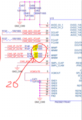
I assume the schematics on both pages are identical; only checked page 25. I did notice several net names were duplicated between schematic pages 25 and 24 that should be different net names. For example, CW_IP_OUTP is used on both schematic pages but should be different net names.
1. Connect thermal pad to ground (GND_CW)
2. SPI_EN, CS, RESET should be pulled up to DVDD_1V8 (D1.8VP) to avoid possible noise coupling into analog section of ADC.
3. SMPL_CLKM should be connected to ADC ground (GND_CW)
4. I do not see any net connections to DCLKM/DCLKP or FCLKM/FCLKP differential pairs.
5. Connect the THS4552 thermal pad to VS (GND_CW)
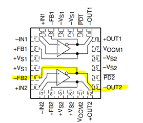
6. There is an error on the THS4552 output connections. The OUT2+ and OUT2- pins are reversed; same for the OUT1+ and OUT1- pins. You do not need to connect the FB and OUT pins together. These are both the same output (-FB2 is the same node as -out2); the OUT pin is used to drive the load (input filter for the ADC) and the FB pin is used for the feedback network. The way the schematic is now drawn, the OUT1+ and OUT1- pins are shorted together; same for OUT2+ and OUT2- pins.
Regards, Keith Nicholas Precision ADC Applications
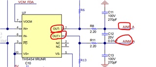
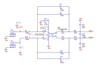
The approximate input/output is shown in the figure above.
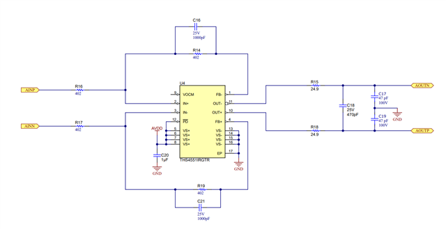
I would like to know the reference of R and C values of THS4552 and ADS9217 input output terminals. There is confusion because the EVM and reference circuit diagram R and C values received from TI are different. Please review it.
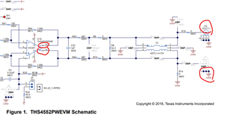
There are multiple variations that will have similar performance. I would suggest using the ADS9218EVM values, since these have been built and tested on multiple hardware.
Suggested schematic for a Gain=1, optimal for input signal frequency up to 100kHz.
Also, the recommended input resistor values between the differential input capacitor (C12 in the EVM schematic) and the ADC inputs is 20Ohm. It appears that you have 50ohm in your schematic; I would suggest changing these values to 20Ohm.
Looking at the details for the AFE5832, it appears that these are current outputs, not voltage. Your external circuit will need to be configured in a TIA configuration to translate this to a voltage. The AFE5832EVM user's guide uses the following amplifier as the first stage current-to-voltage: