This thread has been locked.

If you have a related question, please click the "Ask a related question" button in the top right corner. The newly created question will be automatically linked to this question.

DAC3174: DAC1 and DAC2 analogs' output signals out of sync

Part Number: DAC3174
Other Parts Discussed in Thread: CDCE62005

Hi Team,

My client has a problem:

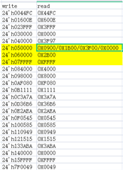
DAC1 and DAC2 analogs' output signals are not synchronous (single-chip with synchronous two-channel output). At present, the DATACLK and DATA signals input by the FPGA to DA1 and DA2 are all in a synchronous alignment state measured on the pins of the DAC chip. The SYNC1 and SYNC2 signals are aligned (pulse rising edge), and the ALIGN1 and ALIGN2 signals are aligned (pulse rising edge) too. There is a phase difference in the analog output. The description in the datasheet about how to use the ALIGN signal is not very clear. If I want to realize the synchronous output of two DACs, is there any modification that I could make?
Specifically, the DAC adopts the default register state mode, NORMAL Dual Sync mode. After power-on, the DAC is reset and then starts working with the default mode.

I read the document https://www.ti.com/lit/an/slaa584/slaa584.pdf, but I still don't know if I want to ensure that there is no difference in DAC analog output, what configuration should I make? Could you offer me any documents for references?

Could you provide technical support?

Kind regards,

Katherine

  • Katherine,

    The part number in this post calls out the DAC3174 but the document you reference calls out the DAC348x. Which part are you having the issue with?

    Regards,

    Jim

  • Hi Jim,

    According to the DAC3174 manual, power-on reset can put the two chips in the synchronous mode.

    Which part are you having the issue with?

    I post this issue for a customer. I'll inquire him and get back to you as soon as possible.

    Regards,

    Katherine

  • Hi Jim,

    but the document you reference calls out the DAC348x

    The customer replied that the document was sent by someone from TI (I don't know who sent it exactly) to him. He said he found it strange as well and asked which part he should refer to. He checked the 3174datahseet and it contained no information that he could check for reference.

    He complained that 4 days had passed since he posted his question and his issue still remained to be solved. He said he would replace it with another chip if there was no solution.

    According to the 3174 manual, the two chips can be synchronized after the power-on and the reset. But after power-on and reset, there was no synchronization. He inquired how to solve it and locate it. And he said that he'd appreciate it if specific solutions could be provided for his questions respectively.

    Besides, could you share any documents for reference so that I could send them to the customer?

    Regards,

    Katherine

  • Katherine,

    How much phase difference is there between DAC's? If it is just one clock cycle, there could be an issue with the input timing that can be adjusted using the delay settings in register 0x03.

    If the phase difference is several clock cycles, they can just the FIFO read start pointer on one device using register 0x09 to shift the output.

    They must use both parts in single bus mode, and both the SYNC and ALIGN input transitions should occur at the same clock cycle on each part.

    Can they swap the data going to the two DAC's from the FPGA to see if this swaps the phase of the analog outputs?  

    Can they send their register settings used?

    Regards,

    Jim 

  • Hi Jim,

    Thanks for your reply.

    The phase difference is several clock cycles, about 3 clock cycles. They both in single bus mode. The rising edge of sync and align is in the same clock cycle. The sync and align signal are period signal or not. If period signal, what is the period. I use fpga give align, but DAC3714 EVB use cdce62005 give align, does it ok?

    Best wishes.

    CHI

  • Hi, Jim

    thank for your reply, and nice to meet u.

    The phase difference is several clock cycles, about 3 clock cycles. They both in single bus mode. The rising edge of sync and align is in the same clock cycle. The sync and align signal are period signal or not. If period signal, what is the period. I use fpga give align, but DAC3714 EVB use cdce62005 give align, does it ok?

    Best withes.

    CHI

  • CHI,

    I would suggest using a pulse for sync and align. The align pulse period would have to be related to the DACCLK in such a way when the pulse occurs, the read pointer always occurs at the same location. This should be referenced to the DACCLK, like it is on the TI EVM. The SYNC should be referenced to the DATACLK.

    Did you try swapping the data going to the two DAC's?

    Regards,

    Jim 

  • Hi,dear Jim,

    It is one and the same data source(sine) sent to two different IOB of fpga, which connected to two DACs through PCB layout trace. if it is still necesssary to make swapping test at the condition, please let me know.

    In addition, I found that for a single DAC, with the same configuration, the delay of the channel is different after each power-up, there is a difference of 3 clock cycles, and even pointer collision.This can be seen from the config5 register。 I don't know if this is normal or if it will be able to provide some positioning information.

    The image below shows the register lists sent to DAC and read information. For example, the register 5 report pointer collision at one certain time when I try to read back after setting. Perhaps it is related to this problem.

  • In more detail,  the power-up timing is  "tx disable-->pull down reset-->write registers-->output sync and align signal" .  I tried to power up several times in a row and got different time delay of path with register5 read back different pointer. It seems the delay of DAC path is not a certain fixed one?  So is the time delay a fixed one?

    CHI

  • CHI,

    I setup the TI EVM and monitored the output of both channels with a 500MHz sample clock going to the DAC and a 45MHz test tone going to both channels. After power and clock is applied to the EVM, I issued a hard reset then loaded the attached config file to the DAC. After several cycles of resending the test pattern, the outputs were always aligned. From reset to reset of the test pattern, the largest delay I saw was 6ns, which is 3 clock cycles. I do not have much history on this part and the designers are no longer with our group so I do not know if this to be expected. I also was getting different values for conf 0x05 as well with each power cycle. I will look into this and see what I can find out.

    Regards,

    Jim 

    7343.dac3174_reg.cfg

  • Hi dear Jim,

    I offer u some information for reference.

    1)There is no difference between the DAC output when the clock period of the Align signal is equal to the DAC clock frequency and 1/8 DAC clock frequency.

    2)According to the manual information, the rising edge of the align signal triggers synchronization (the corresponding channel delay also changes), not the falling edge. In actual tests, it was found that the falling edge triggered the synchronization.

    3)According to the manual information, the digital delay is 26 DAC clocks with no jitter. In the actual measurement, about 3 clock cycles of jitter.

    Thanks 

    CHI

  • Hi, Jim and Katherine,

    i am looking forward to your reply. Perphap you can give same advice or some try action.

    thanks

  • CHI,

    Is it possible to use a single trigger pulse that will do the following:

    1. Start the data going out of the FPGA.

    2. Used as the SYNC and Align inputs to the DAC.

    3. Used to trigger your scope. 

    4. Is synchronized with the DATA CLK. 

    Try this test if you can.

    Is your DATACLK synchronized with DACCLK?

    We currently do not have firmware support for our pattern generator hardware, and the current firmware cannot provide an alignment input to the DAC EVM.

    Have you tried testing with the IOTEST patterns?

    Regards,

    Jim