This thread has been locked.

If you have a related question, please click the "Ask a related question" button in the top right corner. The newly created question will be automatically linked to this question.

ADS1294: Unable to get the ADC values , Test signal & Temperature values

Part Number: ADS1294

Hi

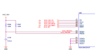
We are working on our custom board of ADS1294CZXGT, We are able to read write the register, but unable to get the test signal , ADC data, Temperature value.

When we set ((MVDD for supply measurement))

CH1SET(0x05) = 0x03h ,

CH2SET(0x05) = 0x03h , 

CH3SET(0x05) = 0x03h , 

CH4SET(0x05) = 0x03h

we get ADC value

0xC0, 0x00, 0x00, 

0x00, 0x00, 0x00, 

0x00, 0x00, 0x00, 

0x28, 0x00, 0x00, 

0x3C, 0x00, 0x00,

Rgds

Chandra

  • Hi,

    Do you have an evaluation kit/board(EVM) so that you may use is as a standard reference to help you debug&troubleshooting?

    in the meantime, make sure to follow the proper power up and reset sequence described in data sheet and take a look of the following for SPI debug&troubleshooting.

    https://e2e.ti.com/support/data-converters-group/data-converters/f/data-converters-forum/775262/faq-ads129x-i-m-having-trouble-communicating-with-my-ads129x-device-via-spi-what-debug-steps-i-should-try/2868427#2868427

    Thanks,

  • Hi 

    We not have evaluation board. 

    As per the document shared we are able to read and write the register. Also we are able to read MVDD voltage from SPI.

    But when we set to read Analog data or Temperature data or Test signal we read all Zeros

    Rgds

    Chandra

  • Hi,

    Without having/using an EVM, it makes it very challenge to guide to debug and troubleshooting.

    --------------------------------------------------------------------

    maybe try take a step back to do some basic tests first -

    0. what are the VREFP, VREFN and VREF = (VREFP – VREFN)?

    1. Try follow the datasheet 11.1 Power-Up Sequencing and this thread to do proper power up and reset

    https://e2e.ti.com/support/data-converters-group/data-converters/f/data-converters-forum/772043/faq-ads129x-why-does-the-device-id-register-show-the-incorrect-number-of-channels

    2. Try to see if you could read 9.6.1.1 ID: ID Control Register (address = 00h) (reset = xxh), correctly?

    3. For test signal,

    "Setting CHnSET[2:0] = 101 provides internally-generated test signals"

    and

    CONFIG2: Configuration Register 2 (address = 02h) (reset = 40h) INT_TEST 1 = Test signals are generated internally

    You may try toggle the following too

    TEST_AMP -

    Test signal amplitude These bits determine the calibration signal amplitude.

    0 = 1 × –(VREFP – VREFN) / 2400 V

    1 = 2 × –(VREFP – VREFN) / 2400 V

    TEST_FREQ[1:0] -

    Test signal frequency These bits determine the calibration signal frequency.

    00 = Pulsed at fCLK / 2^21

    01 = Pulsed at fCLK / 2^20

    11 = At dc

    Thanks

  • Hi 

    Please find my reply below

    0. what are the VREFP, VREFN and VREF = (VREFP – VREFN) 

    2.5Volts

    1. Try follow the datasheet 11.1 Power-Up Sequencing and this thread to do proper power up and reset

    Reset is pulled high(100K pullup & 0.01uF cap connected to gnd). In our case no control .

    2. Try to see if you could read 9.6.1.1 ID: ID Control Register (address = 00h) (reset = xxh), correctly?

    0x90 we are getting

    3. For test signal,

    We tried , but no success.

    Below is our circuit diagram, VCAP1, VCAP2, VCAP3 are shorted together, Is this the cause why we not get ADC data? 

    Rgds

    Chandra

  • Hi

    All VCAPx should not connect to GND directly; connecting to GND may ruin/damage the internal voltage reference buffer and cause ADC conversion not working properly or wrong conversion.

    VCAP1 requires a 22uF to GND as shown in EVM user guide page 53, datasheet page 8, 10, 33 and page 96 11.1 Power-Up Sequencing

    VCAP1 has to be at least or around 1.1V after proper power-up sequencing.

    Thanks

  • Hi,

    VCAPx not shorted to ground in our design. They all shorted together please refer the circuit shared.

    Rgds

    Chandra

  • OK.

    then, next step is to refer to page 96 11.1 Power-Up Sequencing

    Please check whether VCAP1 has at least or around 1.1V after proper power-up sequencing.

    And, the follow 9.5.2.3 RESET: Reset Registers to Default Values to do a RESET.

    -------------------------

    may I ask how many ADS1294 do you encounter this issue?

    and by referring to 9.4.1.1 Start Mode, how did you start the acquisition? START command or START pin to High?

    --------------

    Have you try set MUX[2:0] to 

    000 = Normal electrode input 

    101 = Test signal

    and see if you read any ADC values? 

    Did you try to use oscilloscope to probe on the SPI's DOUT and /DRDY pins?

    Thanks

  • Hi 

    follow 9.5.2.3 RESET: Reset Registers to Default Values to do a RESET. --> Yes we read Default values

    may I ask how many ADS1294 do you encounter this issue? --> Two PCBs having same problem

    101-= Test Signal, we always get value as below,

    I (5294) ads1294: 0 ::: 0xc0
    I (5294) ads1294: 1 ::: 0x00
    I (5304) ads1294: 2 ::: 0x00
    I (5304) ads1294: 3 ::: 0x00
    I (5304) ads1294: 4 ::: 0x00
    I (5314) ads1294: 5 ::: 0x00
    I (5314) ads1294: 6 ::: 0x00
    I (5314) ads1294: 7 ::: 0x00
    I (5324) ads1294: 8 ::: 0x00
    I (5324) ads1294: 9 ::: 0x14
    I (5334) ads1294: 10 ::: 0x00
    I (5334) ads1294: 11 ::: 0x00
    I (5334) ads1294: 12 ::: 0x00
    I (5344) ads1294: 13 ::: 0x00
    I (5344) ads1294: 14 ::: 0x00

    000 = Normal electrode input , we always

    I (5294) ads1294: 0 ::: 0xc0
    I (5294) ads1294: 1 ::: 0x00
    I (5304) ads1294: 2 ::: 0x00
    I (5304) ads1294: 3 ::: 0x00
    I (5304) ads1294: 4 ::: 0x00
    I (5314) ads1294: 5 ::: 0x00
    I (5314) ads1294: 6 ::: 0xfe
    I (5314) ads1294: 7 ::: 0x00
    I (5324) ads1294: 8 ::: 0x30
    I (5324) ads1294: 9 ::: 0x14
    I (5334) ads1294: 10 ::: 0x00
    I (5334) ads1294: 11 ::: 0x00
    I (5334) ads1294: 12 ::: 0x00
    I (5344) ads1294: 13 ::: 0x00
    I (5344) ads1294: 14 ::: 0x00

    Below is the register set values, read and write working correctly

    void ads1294_test_init(void)
    {
    uint8_t value[1] = {0x00};
    ads1294_stop_cread();

    ads1294_read(ADS1294_CONFIG4_READ,&value[0]);
    ads1294_write(ADS1294_CONFIG4_WRITE,0x0E);
    ads1294_read(ADS1294_CONFIG4_READ,&value[0]);

    ads1294_read(ADS1294_CONFIG3_READ,&value[0]);
    ads1294_write(ADS1294_CONFIG3_WRITE,0xC0);
    ads1294_read(ADS1294_CONFIG3_READ,&value[0]);

    ads1294_read(ADS1294_CONFIG1_READ,&value[0]);
    ads1294_write(ADS1294_CONFIG1_WRITE,0x86);
    ads1294_read(ADS1294_CONFIG1_READ,&value[0]);

    ads1294_read(ADS1294_CONFIG2_READ,&value[0]);
    ads1294_write(ADS1294_CONFIG2_WRITE,0X10);
    ads1294_read(ADS1294_CONFIG2_READ,&value[0]);

    ads1294_read(ADS1294_CH1SET_READ,&value[0]);
    ads1294_write(ADS1294_CH1SET_WRITE,0X05);
    ads1294_read(ADS1294_CH1SET_READ,&value[0]);

    ads1294_read(ADS1294_CH2SET_READ,&value[0]);
    ads1294_write(ADS1294_CH2SET_WRITE,0X05);
    ads1294_read(ADS1294_CH2SET_READ,&value[0]);

    ads1294_read(ADS1294_CH3SET_READ,&value[0]);
    ads1294_write(ADS1294_CH3SET_WRITE,0X05);
    ads1294_read(ADS1294_CH1SET_READ,&value[0]);

    ads1294_read(ADS1294_CH4SET_READ,&value[0]);
    ads1294_write(ADS1294_CH4SET_WRITE,0X05);
    ads1294_read(ADS1294_CH4SET_READ,&value[0]);
    }

    main (void)
    {
    ads1294_soft_restart(); // added this we see CH2 some value which is decreasing from 0xff, 0x00, 0x00 & in CH3 , 0x14, 0x00, 0x00
    delay(10); //10ms delay
    ads1294_start_gpio(1);
    ads1294_start_data();
    delay(10); //10ms delay
    ads1294_start_cread();
    delay(10); //10ms delay
    }

    Rgds

    Chandra

  • Hi,

    What are VCAPx voltage measured?

    Do you use internal reference or external reference?

    What are the CLK and SCLK frequency? Make sure CLK and SCLK meet the requirement described in datasheet -7.6 Timing Requirements: Serial Interface

    -----------------------------------------------------------------------------

    Next further step is to use oscilloscope(large memory) to probe all the SPI signals lines, and please use/refer to datasheet Figure 1. Serial Interface Timing and Figure 71. RDATA Usage and this e2e

    https://e2e.ti.com/support/data-converters-group/data-converters/f/data-converters-forum/775262/faq-ads129x-i-m-having-trouble-communicating-with-my-ads129x-device-via-spi-what-debug-steps-i-should-try/2868427#2868427

    to see if you can see whether the /CS, DIN, START, DOUT behave correctly?  It's suggested to use an EVM as a reference/comparison.

    Thanks 

  • HI

    What are VCAPx voltage measured? - 4.1 Volts apx we are getting

    Do you use internal reference or external reference? - Internal Reference

    What are the CLK and SCLK frequency? - CLK = 2.048Mhz internal, SCLK = 4Mhz

    Make sure CLK and SCLK meet the requirement described in datasheet -7.6 Timing Requirements -> Yes we are meeting the requirement. We are able to read and write registers.

  • Hi,

    What is the register you wrote to CONFIG3: Configuration Register 3 (address = 03h) ?

    Particular the VREF_4V bit?

    Note-

    VREF_4V Reference voltage -

    This bit determines the reference voltage, VREFP.

    0 = VREFP is set to 2.4 V

    1 = VREFP is set to 4 V (use only with a 5-V analog supply)

    --------------------------------------------------------------------------

    Is your AVDD 3V? and unipolar?

    ----------------------------------------------------

    Do you tie all VCAPs together?

    Thanks

  • Hi

    What is the register you wrote to CONFIG3: Configuration Register 3 (address = 03h) ? --> 0xC0

    Is your AVDD 3V? and unipolar? -- Yes

    Do you tie all VCAPs together? -- Yes

    Rgds

    Chandra

  • Hi,

    Please check the datasheet and EVM schematic, VCAPs cannot be tied together.

    Thanks