This thread has been locked.

If you have a related question, please click the "Ask a related question" button in the top right corner. The newly created question will be automatically linked to this question.

DAC53004: OUT voltage saturates at 1.8V even though 0V is asked (force-sense configuration with MOSFET)

Part Number: DAC53004

Hello,

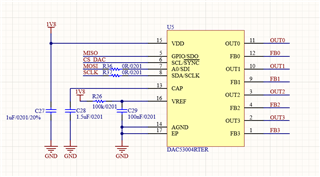
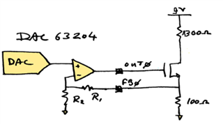
I am using the DAC53004 to control the current in a load with a force-sense configuration with a MOSFET:

We are doing pulses of 50us/250us, with about 20ms rest in-between. During the resting, 0 is sent to registers DAC-X-DATA (19h, 1Ah, 1Bh, 1Ch).

The gain is 1.5 and the reference used is 1.21V.

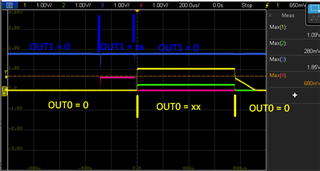
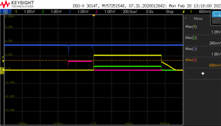
The problem is, sometimes in one of the channel OUT I can see 1.8V during the resting time, instead of 0V. It saturates for some reason.

This is what I am seeing. Blue is OUT1 and Pink is FB1. Yellow is OUT0 and Green is FB0.

The OUT0/FB0 is what I am expecting, and the OUT1/FB1 is what is going wrong.

Do you have an explanation for that?

Best Regards,

Aurélie

  • Hi Aurélie,

    Please share a full schematic with the resistance values for each FET on each channel shown. Can you also label your screenshot to show when DAC-0 and DAC-1 data are being changed to different values? 

    You said that OUT0/FB0 is what is expected, but FB0 is not 0 during the reset which means the current through the load is also not 0. Is that what is expected? 

    Best,

    Katlynne Jones 

  • Hi Katlynne,

    Here is the schematic:

    And here is the screenshot with labels:

    The pulses induced by OUT0 and OUT1 don't overlap, we have first the pulse induced by OUT1 and then the pulse induced by OUT0.

    Best Regards,

    Aurelie

  • Hi Aurelie,

    Where is the 1300R load connected in the schematic? 

    Best,

    Katlynne Jones 

  • Hi Katlynne,

    The 1300R is connected between E1 and E2.

    Best Regards,

    Aurelie

  • Hi Aurelie,

    I understand. So depending on which DAC channel is pulsing, you are attempting to change the direction of the current through the load. Is that right? 

    I mentioned in one of my other responses that the OUTx pin of whichever channel adjusts so that the FBx pin of that channel equals the setpoint set in the DAC-X-DATA register. When Q3 is switched off and the 9-V to channel 1 is removed, what is the drain voltage on Q6? What is the drain voltage on Q5 when Q2 is removed? It looks like both FBx voltages are at 0V when they should be, so it's possible that there is some steady state response in the circuit with the pulses that is causing OUT0 to need to change, but OUT1 to stay constant to achieve the desired setpoint on FBx. This could also be why you are seeing the ramp down on OUT0. Are you setting the DAC-X-DATA registers for each channel to the same value or different value when OUT0=xx and OUT1=xx on the scope plot? 

    Best,

    Katlynne Jones